TOPFAST PCB One-Stop Solutions

Blog

PCB Conformal Coating

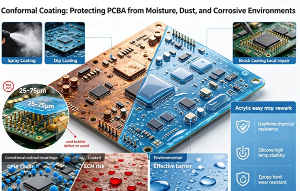
Conformal Coating: Protecting PCBA from Moisture, Dust, and Corrosive Environments

Introduction to Conformal Coating in PCB Assembly In the realm of high-reliability printed circuit board assembly (PCBA), protecting the intricate web of traces, vias, and delicate surface-mount technology (SMT) components is not merely an option, but a strict engineering mandate. Conformal coating is a thin, polymeric film applied directly to the PCBA surface, contouring precisely […]
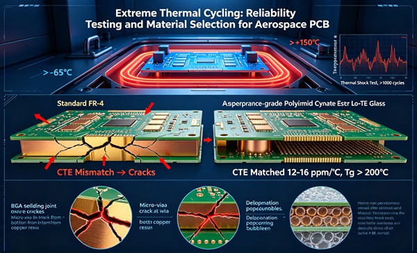
Extreme Thermal Cycling

Extreme Thermal Cycling: Reliability Testing and Material Selection for Aerospace PCBs

The harsh environment of aerospace applications presents unparalleled challenges for electronics. From the unforgiving vacuum of Low Earth Orbit (LEO) to the high-friction descent of reentry vehicles, aerospace printed circuit boards (PCBs) must endure extreme environmental stressors. Among the most destructive of these stressors is extreme thermal cycling—the rapid and repeated fluctuation of temperatures across […]

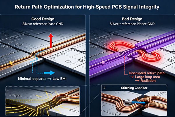
Return Path Optimization

Return Path Optimization: Designing Solid Reference Planes for High-Frequency Signal Integrity

In the realm of advanced printed circuit board (PCB) design, engineers often focus heavily on the routing of signal traces—meticulously tuning lengths, matching impedances, and routing differential pairs with extreme precision. However, a signal trace is only one half of the electrical equation. Every electrical signal requires a complete closed loop to flow, meaning the […]

Skew Compensation

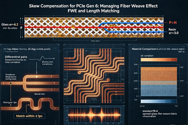
Skew Compensation: Managing Fiber Weave Effect (FWE) and Length Matching for PCIe Gen 6

Introduction to PCIe Gen 6 Signal Integrity Challenges The transition to Peripheral Component Interconnect Express (PCIe) Generation 6 introduces unprecedented challenges in high-speed printed circuit board (PCB) design. Operating at 64 GigaTransfers per second (GT/s) and utilizing Pulse Amplitude Modulation 4-level (PAM4) signaling, PCIe Gen 6 demands stringent signal integrity (SI) management. PAM4 encodes two […]

PCB Crosstalk Mitigation

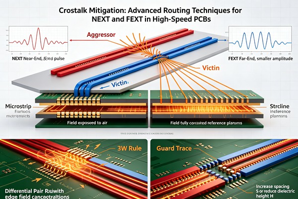
Crosstalk Mitigation: Advanced Routing Techniques to Minimize NEXT and FEXT in High-Speed PCBs

Understanding Crosstalk in High-Speed PCB Design In the realm of high-speed Printed Circuit Board (PCB) design, signal integrity is paramount. As data rates climb into the multi-gigabit per second (Gbps) range and edge rates become progressively faster, electromagnetic coupling between adjacent traces becomes a critical concern. This phenomenon, known as crosstalk, can lead to data […]

M-SAP Technology

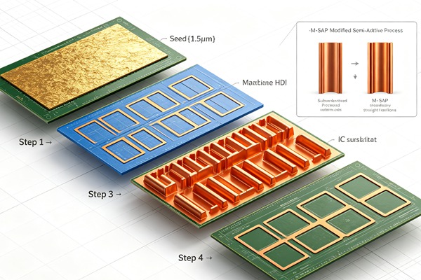
M-SAP Technology: Achieving Sub-25 Micron Line/Space for Next-Generation Electronics

The relentless march of miniaturization in the electronics industry demands continuous innovation in Printed Circuit Board (PCB) manufacturing. As semiconductor nodes shrink and package sizes condense, the underlying substrate and PCB must keep pace. Enter M-SAP technology—the Modified Semi-Additive Process. This advanced manufacturing technique has emerged as the critical enabler for High-Density Interconnect (HDI) boards […]

1 2 56