Table of Contents
Introduction to Probe Cards in Semiconductor Testing
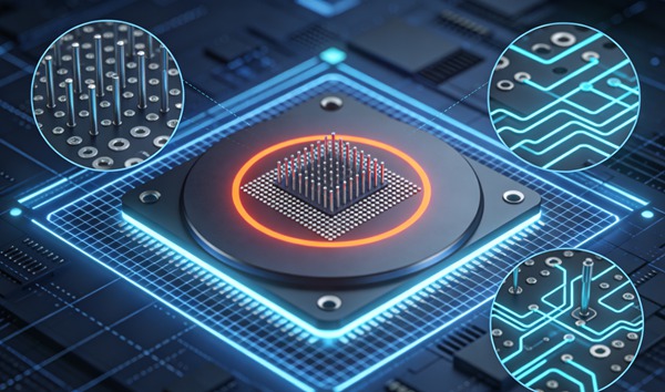
In the fiercely competitive landscape of semiconductor manufacturing, ensuring the reliability and functionality of integrated circuits (ICs) before packaging is an absolute necessity. Probe cards serve as the critical electro-mechanical interface between the Automated Test Equipment (ATE) and the bare semiconductor wafer. Operating as the fundamental translation layer, a probe card must maintain pristine signal integrity, manage substantial power loads, and provide pinpoint mechanical accuracy across thousands of microscopic contact pads.
The rapid evolution of microelectronics—characterized by relentless node shrinking, the rise of chiplet architectures, and the proliferation of heterogeneous integration (such as 2.5D and 3D packaging)—has pushed traditional printed circuit board (PCB) technologies to their absolute limits. As I/O counts skyrocket into the tens of thousands per die, designing and manufacturing multi-layer test interface boards for probe cards is one of the most demanding disciplines in PCB engineering today. These complex interface boards routinely feature upwards of 40 to 60 layers, intricate microvia structures, and highly specialized dielectric materials engineered for microwave-frequency performance and exceptional thermal stability.
Test engineers, hardware designers, and PCB fabrication specialists tasked with validating the next generation of advanced semiconductor devices need a deep understanding of the engineering principles behind these multi-layer test interface boards.
The Architecture of a Probe Card System
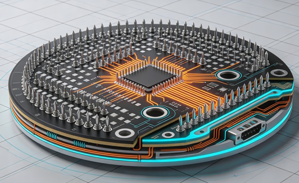
A standard advanced probe card assembly is not a monolithic component; rather, it is a highly sophisticated, modular system comprising several integrated elements:
- The Probe Array (Contact Contactor): The physical needles, bumps, vertical springs, or MEMS (Micro-Electro-Mechanical Systems) structures that make direct, physical contact with the aluminum or copper die pads on the wafer.
- The Space Transformer (MLC or MLO): Often a Multi-Layer Ceramic (MLC) or Multi-Layer Organic (MLO) substrate. This component “transforms” the ultra-fine pitch of the probe array (sometimes sub-50 microns) to a more manageable, albeit still dense, pitch on the main Printed Circuit Board (PCB).
- The Multi-Layer Test Interface Board (PCB): The robust, primary PCB that routes thousands of signals from the space transformer to the ATE tester connections (such as high-density pogo pin pads, cable assemblies, or specialized edge connectors). It handles power distribution, complex signal conditioning, and provides a rigid mounting platform.
- Mechanical Stiffeners and Hardware: Structural components made of stainless steel or specialized alloys, critical for maintaining the planar integrity of the PCB under the extreme, repeated compressive forces exerted during the wafer probing process.
Design Challenges in Multi-Layer Test Interface Boards
The design of the main PCB within a probe card assembly is an exercise in solving a highly constrained, multi-physics matrix involving electrical, mechanical, and thermal variables.
Signal Integrity and High-Frequency Routing
Modern integrated circuits, particularly those designed for 5G/6G RF communications, High-Performance Computing (HPC), and advanced GPU applications, operate at extraordinarily high frequencies and multi-gigabit data rates. The test interface board must transmit these ultra-fast signals without signal distortion, attenuation, jitter, or cross-talk.
Design engineers must enforce stringent impedance control—typically 50 ohms single-ended and 85 to 100 ohms differential—across all high-speed signal traces. This mandates the precise calculation of trace widths, inter-layer dielectric thicknesses, and copper weights. The strategic implementation of blind, buried, and staggered microvias is critical to minimize via stubs. These stubs act as unwanted resonant antennas, heavily degrading signal quality at gigahertz frequencies. Furthermore, massive ground shielding, co-planar waveguide structures, and optimized return path configurations are absolutely mandatory to isolate highly sensitive RF or analog signals from aggressively switching, noisy digital logic lines. Learn more about Nitrogen Reflow Soldering: Improving Solder Wetting in Lead-Free PCBA.
Power Integrity and Current Delivery
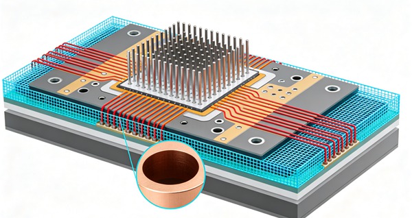
High-performance server processors and AI accelerators demand colossal amounts of power—frequently exceeding several hundreds of amps—delivered at extremely low core voltages (sub-1V). Under these conditions, the probe card PCB must function as a hyper-efficient, low-impedance power delivery network (PDN).
Design strategies heavily rely on allocating multiple thick-copper layers (often 2 oz to 4 oz) entirely dedicated to contiguous power and ground planes. To combat high-frequency power supply noise and transient voltage droop, bypass and decoupling capacitors must be placed with extreme precision. They are frequently mounted directly adjacent to the space transformer interface or embedded completely within the internal PCB layers to drastically minimize parasitic loop inductance.
Extreme Density and Layer Counts
To effectively accommodate the thousands of individual test channels required by state-of-the-art ATE platforms, test interface boards continually redefine the boundaries of conventional PCB density. It is standard for these highly complex boards to utilize 30 to 60 independent copper layers.
Routing such staggering pin counts necessitates advanced HDI (High Density Interconnect) topologies. This involves utilizing any-layer via structures, extremely fine lines and spaces (often dropping below 3 mil / 75 microns), and enormous via-in-pad arrays to manage the dense BGA or LGA interface to the space transformer.
Mechanical Rigidity, Planarity, and Thermal Management
During the automated wafer test cycle, the probe card is aggressively pressed against the silicon wafer with immense mechanical force (often hundreds of kilograms in total) to ensure reliable ohmic contact across all thousands of probes simultaneously. Any deflection, bowing, or warping of the PCB will immediately result in uneven probe pressure. This can lead to false test failures, physically damaged wafer pads, or catastrophic wafer cracking.
The PCB design must heavily incorporate ultra-high-Tg (glass transition temperature) materials that resist thermo-mechanical warpage. Symmetric layer stack-ups are mathematically calculated to balance internal lamination stress. Furthermore, specialized thermal management solutions—such as heavy copper planes acting as heat spreaders and strategic thermal vias—are employed to dissipate the localized heat generated by testing high-power dies, ensuring the board’s structural integrity remains intact under continuous thermal cycling.
Advanced Materials for Probe Card PCBs
The extreme electrical and mechanical demands of probe card applications absolutely preclude the use of standard, off-the-shelf FR-4 fiberglass materials. Specifying the correct advanced dielectrics and highly refined conductive materials is arguably the most critical engineering decision in the design phase. Learn more about Cavity PCBs: Designing Recessed Cavities for RF Power Amplifiers.
- High-Frequency Laminates: Advanced PTFE (Teflon) blends, thermoset hydrocarbon resins (like the Rogers RO4000 series), or high-speed polyphenylene ether (PPE) blends (such as Panasonic Megtron 6 or 7) are heavily utilized. These laminates offer exceptionally low dielectric constants (Dk) and ultra-low dissipation factors (Df), ensuring minimal signal loss and phase delay at microwave frequencies.
- High-Tg and Low-CTE Dielectrics: Polyimide or specially formulated epoxy resin systems boasting a high Glass Transition Temperature (Tg > 250°C) and a highly stable, low Coefficient of Thermal Expansion (CTE) are crucial. These specialized properties guarantee that the multi-layer board maintains its strict mechanical dimensional accuracy over hundreds of thousands of thermal test cycles.
- Low-Profile Copper Foils: Standard copper foil possesses microscopic surface roughness that exacerbates the “skin effect” at high frequencies, dramatically increasing conductor loss. Therefore, ultra-low-profile (ULP) or reverse-treated copper foils (RTF) are strictly mandated to optimize the high-frequency signal path.
- Surface Finishes: ENIG (Electroless Nickel Immersion Gold) or ENEPIG (Electroless Nickel Electroless Palladium Immersion Gold) are the industry standards. They deliver exceptional surface planarity, unmatched oxidation resistance, and reliable metallurgical surfaces for both wire bonding interfaces and high-cycle ATE pogo pin contact. Deep hard gold plating is also frequently applied directly to the ATE contact pads to survive the abrasive wear of continuous production testing.
Manufacturing Complexities and Tolerances
Successfully fabricating a massive 50-layer, highly dense test interface board requires pushing the absolute boundaries of modern PCB manufacturing capabilities.
Precision Registration and Scaling
The single greatest challenge in producing ultra-thick, high-layer-count HDI boards is maintaining perfect layer-to-layer registration. With dozens of sequential lamination cycles, the physical movement, shrinkage, and scaling of the dielectric materials must be mathematically predicted and dynamically compensated for with sub-mil accuracy. Top-tier manufacturers utilize state-of-the-art optical alignment systems (such as Direct Imaging), highly specialized inductive pinning techniques, and real-time X-ray imaging metrology to ensure microvias align flawlessly across all inner layers. A misregistration of just fractions of a mil can instantly ruin high-speed signal integrity or create fatal internal shorts. Learn more about Under-Stencil Cleaning: Best Practices for Fine-Pitch SMT Printing.
High Aspect Ratio Plating
Thick test interface boards (frequently exceeding 0.250 inches or 6.35 mm in total thickness) still require critical through-holes for heavy power and ground delivery. Plating a continuous, uniform, and robust copper wall inside a high aspect ratio through-hole (sometimes exceeding 20:1) is an exceptionally difficult electrochemical process. It mandates the use of proprietary chemical plating baths, precision fluid dynamics, and complex Periodic Pulse Reverse (PPR) plating rectifiers. These techniques are required to aggressively push copper ions deep into the barrel while preventing “dog-boning”—the excessive buildup of copper at the surface hole entrance.
Backdrilling (Controlled Depth Drilling)
To physically eliminate the resonant via stubs that destroy high-speed signal integrity, backdrilling is routinely and heavily employed. This process requires massive, highly specialized CNC drilling machines equipped with real-time, precision depth-control sensors. These machines drill out the unused, conductive portion of a plated through-hole without penetrating or damaging the critical inner-layer connection. In advanced probe card designs, this painstaking process must be successfully executed on tens of thousands of individual vias per board, with depth tolerances tightly controlled to within a few thousandths of an inch. Learn more about PTFE (Teflon) PCBs: Manufacturing and Plating Challenges for High-Frequency Boards.
How to Design a High-Performance Probe Card Interface Board (Step-by-Step Guide)
Follow these engineering rules.
- Define the System Architecture and Stack-up
Commence by establishing a close collaboration with the semiconductor test engineers and the specific ATE platform specifications to define the total I/O channel count, necessary RF frequency bandwidth, and stringent power delivery requirements. Formulate an initial, highly detailed layer stack-up utilizing specialized high-speed/low-CTE laminates. Carefully allocate dedicated, shielded routing layers for signals, interspersed with heavy-copper planes for power and ground to guarantee optimal return paths.
- Establish Impedance Rules and Via Structures
Perform complex electromagnetic calculations to determine the exact trace geometries required to meet strict single-ended and differential impedance targets. Concurrently, define the entire via architecture—specifying precisely where standard plated through-holes, mechanically drilled blind/buried vias, and laser-drilled microvias will be deployed to support the extreme routing density while strictly minimizing high-frequency stubs.
- Design the Power Delivery Network (PDN)
Run exhaustive pre-layout simulations on the proposed PDN. Ensure it can robustly handle the maximum transient current draw with absolute minimal IR voltage drop and minimal target impedance at high frequencies. Strategically place high-value bulk capacitors and ultra-low ESL (Equivalent Series Inductance) high-frequency decoupling capacitors on the top and bottom board surfaces.
- Execute High-Density Routing
Route the most critical, highest-speed RF and digital signal lines first. This routing must adhere to strict length-matching, phase-matching, and aggressive spacing constraints to effectively mitigate crosstalk. Following the critical signals, route the immense power and ground connections, maximizing copper pour topologies to significantly enhance both current carrying capacity and thermal heat dissipation. Finally, route the lower-speed digital control lines and auxiliary utility signals.
- Perform Comprehensive Signal Integrity Analysis
Utilize advanced 3D electromagnetic (EM) field solvers and comprehensive SI/PI simulation software suites (such as Ansys HFSS, Keysight ADS, or Cadence Sigrity) to thoroughly analyze all critical signal paths. Validate eye diagrams, TDR (Time Domain Reflectometry) responses, S-parameters (insertion loss and return loss), and comprehensive crosstalk matrices. Iteratively adjust the layout routing and stack-up geometry based on these rigorous simulation results until all electrical performance criteria are definitively met.
- Design for Manufacturability (DFM) and Assembly
Conduct a highly thorough DFM review in direct, continuous coordination with the specific PCB fabricator chosen to build the board. Verify that all annular rings, drill sizes, plating aspect ratios, and trace/space clearances strictly comply with their specialized capabilities for ultra-thick, high-layer-count HDI boards. Explicitly define all mechanical stiffener mounting locations and specify the critical coplanarity tolerances required for the final assembly.
Designing an advanced multi-layer test interface board requires an incredibly methodical, simulation-driven approach to successfully manage its inherent complexity.
Conclusion
The engineering required to design and manufacture probe cards and multi-layer test interface boards stands as a testament to the absolute extremes of modern PCB technology. As next-generation semiconductor architectures continue to aggressively scale down in node size while adopting highly complex 2.5D and 3D heterogeneous packaging, the physical and electrical demands placed on the test interface will only intensify. Achieving success in this highly specialized field requires a deep, multi-disciplinary integration of high-speed electrical design, advanced materials science, and a comprehensive mastery of cutting-edge fabrication techniques. This ensures that the highly sophisticated microchips of tomorrow can be reliably and accurately tested in the high-volume production environments of today.
Frequently Asked Questions (FAQ)
The space transformer acts as an essential pitch translation device. It electrically connects the ultra-fine, dense pitch of the microscopic probe array (which makes direct contact with the silicon wafer) to the much larger, standard manufacturing pitch of the multi-layer test interface board. This translation allows for practical, manufacturable PCB routing.
Standard FR-4 glass-epoxy lacks the superior high-frequency electrical performance—exhibiting a higher dielectric constant (Dk) and dissipation factor (Df)—required for transmitting modern, multi-gigabit test signals without severe loss. Furthermore, FR-4’s physical properties, particularly its higher Coefficient of Thermal Expansion (CTE), can lead to mechanical instability and severe board warpage under the extreme temperatures and compressive stresses of wafer probing.
When a via does not need to span the entire thickness of a board to make its connection, the unused, leftover portion of that plated hole (the stub) acts as an open-ended, resonant antenna. This stub reflects high-frequency signals back upon themselves, severely degrading signal integrity and closing the data “eye.” Backdrilling physically machines away this conductive stub, significantly improving the transmission characteristics of high-speed data channels.
While simple parametric or low-density test boards might only utilize 10 to 20 layers, highly complex test interface boards designed for modern multi-core CPUs, GPUs, or high-density memory arrays routinely range from 30 to well over 50 layers. This massive layer count is mandatory to accommodate the staggering pin counts and the highly complex, dedicated power delivery networks required.
During automated testing, thousands of microscopic probes must make simultaneous, uniform electrical contact with the microscopic pads on the wafer. If the underlying PCB is warped, bowed, or uneven, some probes will apply excessive pressure (potentially crushing the wafer pads), while others will fail to make any contact at all, resulting in disastrous false test failures. Extreme planarization ensures a uniform, predictable contact force across the entire multi-thousand pin array.