As electronic devices continue to shrink in physical size while expanding in functionality, printed circuit board (PCB) design and assembly must rapidly evolve to accommodate higher component densities. The driving force behind the next generation of wearables, medical implants, and advanced mobile telecommunications is extreme miniaturization. At the forefront of this revolution is the 0201m (metric) component, also known by its imperial designation, 008004. Measuring a microscopic 0.25 mm by 0.125 mm, the 0201m package represents a monumental leap in surface mount technology (SMT).
Transitioning to 0201m components is not merely a matter of scaling down existing processes. It introduces entirely new paradigms in physics, mechanics, and material science on the shop floor. From the structural integrity of the solder paste to the microscopic precision required by pick-and-place nozzles, successfully assembling these ultra-miniature devices demands stringent process control, state-of-the-art capital equipment, and a deep understanding of sub-millimeter manufacturing dynamics. This article explores the core engineering challenges, necessary equipment upgrades, and systematic methodologies required to achieve high-yield 0201m component placement in modern SMT assembly.
Table of Contents
The Evolution of SMD Miniaturization
To understand the magnitude of the 0201m challenge, one must look at the historical trajectory of Surface Mount Device (SMD) packaging. In the early 2000s, the 0402 (imperial) package was considered state-of-the-art. Soon after, the 0201 (imperial) and 01005 (imperial) packages became the standard for high-density interconnect (HDI) applications like smartphones and tablets. Learn more about Busbar PCBs: Integrating Copper Busbars for High-Current Applications.
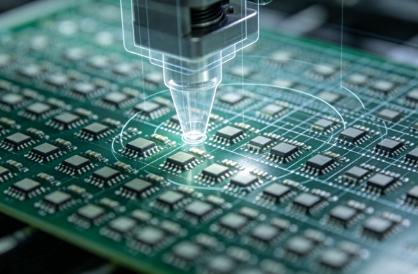
The 0201m (008004) represents a 50% reduction in linear dimensions and a 75% reduction in volume and mounting area compared to the 01005 package. To put this in perspective, a single 0201m capacitor is roughly the size of a grain of fine sand or the diameter of a human hair. Handling components of this scale fundamentally changes how engineers approach printed circuit board assembly (PCBA), pushing the absolute limits of current electromechanical and optical systems.
Engineering Challenges in 008004 Assembly
Implementing 0201m technology introduces a multitude of unique engineering hurdles that require robust solutions: Learn more about Burn-In Boards: High-Density Blind/Buried Vias for High-Pin Count Devices.
- Solder Paste Rheology and Release: At the 008004 scale, the volume of solder paste required is incredibly minute. The physical properties of the solder paste (rheology) must be precisely tuned to allow consistent release through ultra-thin stencils. Standard Type 4 or Type 5 pastes are insufficient; Type 6 or even Type 7 solder pastes with specialized fluxes are mandatory to prevent bridging and ensure adequate wetting.
- Stencil Fabrication Tolerances: Traditional laser-cut stainless steel stencils often lack the smoothness and precision required for 0201m apertures. Electroformed stencils or laser-cut stencils with nanocoatings are required to achieve the necessary area ratios for consistent paste transfer efficiency.
- Placement Accuracy: Pick-and-place machines must reliably achieve placement accuracies of ±10 micrometers (µm) or better at 3 Sigma. Any mechanical vibration, thermal expansion in the machine chassis, or slight PCB warpage will result in fatal placement offsets.
- Tombstoning and Billboarding: Because of the extremely low mass of 0201m components, they are highly susceptible to the surface tension of the molten solder during reflow. Uneven thermal distribution or asymmetrical paste deposits will cause the component to stand on one end (tombstoning) or flip on its side (billboarding).
- Static Electricity (ESD): At micro-scales, electrostatic forces can easily rival gravitational forces. Components can literally jump out of their carrier tape pockets or cling to the side of the placement nozzle due to static charge, making ionization and strict ESD controls critical throughout the assembly line.
How to Master 0201m Placement (Step-by-Step Guide)
Follow these engineering rules.
- Advanced PCB Pad Design and Mask Tolerancing
The foundation of successful extreme miniaturization lies in the bare printed circuit board. Traditional IPC standard pad geometries must be rigorously modified. Non-Solder Mask Defined (NSMD) pads are typically preferred to control the exact solderable area, but the registration tolerance of the solder mask becomes paramount. If the solder mask web between pads is too thin, it may peel and cause bridging. Pad dimensions must be perfectly symmetrical to balance the surface tension forces during reflow, mitigating the risk of tombstoning.
- Solder Paste Printing Optimization
The printing process accounts for over 60% of all SMT defects, and this percentage increases with 008004 components. You must utilize a highly stable, rigid solder paste printer equipped with advanced vision alignment. Implement electroformed stencils with thicknesses ranging from 30 µm to 50 µm, depending on the mixed technology requirements of the board. Utilize Type 6 (or Type 7) solder paste. Ensure the squeegee pressure and speed are optimized to roll the paste efficiently and fill the microscopic apertures completely. Regular under-stencil cleaning is non-negotiable, often required after every single print stroke.
- High-Precision Pick-and-Place Machine Calibration
Standard pick-and-place machines cannot handle 0201m components. You must invest in advanced placement platforms featuring linear motor drives, high-resolution optical encoders, and extreme thermal stability. Before running production, the machine must undergo rigorous calibration using glass plates to map and compensate for any dynamic non-linearities in the X, Y, and Z axes. The vision system must have sub-pixel resolution capabilities to accurately identify the center and orientation of the component on the fly.
- Component Feeding and Nozzle Selection
The packaging of 0201m components is typically 4mm wide carrier tape with 1mm pitch pockets. The feeders must index this tape with zero vibration to prevent components from bouncing out of the pockets before the nozzle arrives. Feeder advancement must be incredibly smooth. Furthermore, specialized ceramic or composite nozzles with microscopic internal diameters are required. These nozzles must be meticulously maintained and regularly inspected for wear or contamination, as even a microscopic dust particle can obstruct the vacuum and cause mispicks.
- Reflow Soldering Profiling for Ultra-Miniature SMDs
The reflow profile must be perfectly balanced. An excessively rapid ramp rate will cause the flux to outgas violently, blowing the ultra-light 0201m components off their pads. A carefully controlled linear ramp-to-spike profile, often utilizing an inert nitrogen atmosphere (N2) with less than 500 ppm of oxygen, is highly recommended. The nitrogen environment significantly reduces oxidation on the micro-pads, improves solder wetting, and lowers the surface tension of the molten solder, which drastically reduces the incidence of tombstoning and voiding.
- Automated Optical Inspection (AOI) and Quality Control
Post-reflow inspection requires ultra-high-resolution 3D AOI systems. Traditional 2D cameras lack the depth perception and resolution necessary to inspect the minute fillets of a 0201m solder joint. 3D AOI utilizing phase-shift profilometry or laser triangulation can accurately measure the volume of the solder joint, check for co-planarity, and identify billboarding or micro-solder balls that would otherwise go unnoticed. Continuous feedback loops from the AOI back to the screen printer and pick-and-place machine are essential for real-time process correction.
Achieving reliable, high-yield assembly with 0201m components requires a systematic approach, analyzing and optimizing every discrete step of the SMT line. Learn more about Nitrogen Reflow Soldering: Improving Solder Wetting in Lead-Free PCBA.
Enhancing Process Stability and Yield
While the steps above define the core implementation, maintaining high yields in a high-volume manufacturing (HVM) environment requires continuous monitoring. Tooling and environmental conditions play an outsized role in the 008004 assembly process.
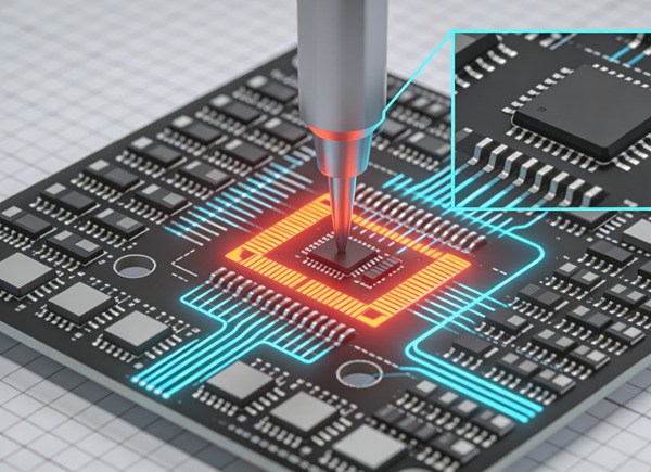
Temperature and humidity controls in the SMT facility must be exact. Variations in ambient humidity can alter the viscosity and tackiness of the micro-solder paste deposits, leading to inconsistent component adherence during the transfer from the pick-and-place machine to the reflow oven.
Furthermore, the mechanical support of the PCB during printing and placement cannot be overlooked. Any flex or bounce in the board during the placement stroke will cause the component to slide off the microscopic paste deposit. Dedicated, custom-machined tooling blocks or high-density support pin matrices are required to ensure the PCB remains perfectly flat and rigid throughout the assembly process. Learn more about RF PCB Design: Impedance Matching and Dielectric Loss Control with Rogers Materials.
The Future of Extreme Miniaturization
The successful adoption of the 0201m package is not the end of the road; it is merely the current frontier. As silicon dies continue to shrink and packaging technologies like System-in-Package (SiP) and heterogeneous integration become more prevalent, the demand for even smaller discrete passive components will inevitably arise.
The lessons learned and the equipment developed for 008004 assembly—sub-micron motion control, Type 7 solder pastes, nanocoated electroformed stencils, and nitrogen-infused thermal profiling—are laying the groundwork for whatever comes next. Electronics manufacturers who master 0201m placement today are securing their position as industry leaders, capable of designing and assembling the next generation of highly complex, ultra-compact electronic devices.
Frequently Asked Questions (FAQ)
The 0201m (metric) or 008004 (imperial) component measures approximately 0.25 mm in length and 0.125 mm in width. The thickness can vary slightly depending on the component type (resistor, capacitor), but is typically around 0.125 mm.
No. Type 4 solder paste has particle sizes that are too large for the microscopic stencil apertures required for 0201m components. Using Type 4 will result in poor paste release, insufficient volume, and bridging. Type 6 or Type 7 solder pastes are strictly required for reliable extreme miniaturization assembly.
While it is technically possible to reflow in an air environment, a nitrogen atmosphere is highly recommended and practically essential for high-yield production. Nitrogen reduces oxidation, improves wetting, and modifies the surface tension of the solder, drastically reducing defects like tombstoning that plague ultra-low-mass components.
Nozzles for 008004 components are significantly smaller and often made from advanced ceramics rather than steel or standard plastics to prevent static buildup and wear. They must have incredibly tight manufacturing tolerances to ensure the vacuum seal is perfect without crushing the fragile component.
Tombstoning in 0201m assembly is primarily caused by unequal surface tension forces on the two ends of the component during the reflow stage. This can be caused by asymmetrical pad design, uneven solder paste volume, or uneven heating. It can be prevented by using perfectly symmetrical pad geometries, optimizing the printing process for exact volume consistency, and using a gradual, controlled thermal profile, ideally in a nitrogen environment.