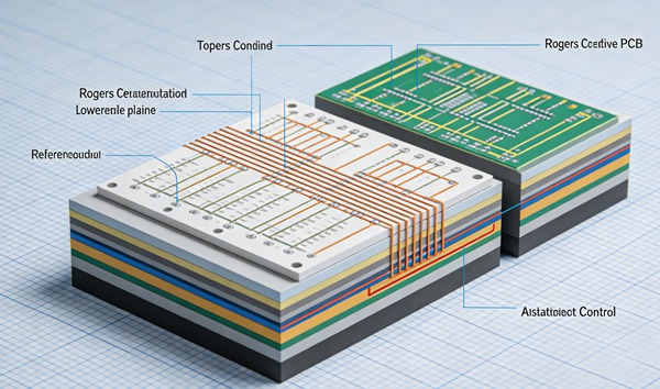
Designing Radio Frequency (RF) and microwave Printed Circuit Boards (PCBs) is widely considered one of the most demanding and unforgiving disciplines in modern electronics engineering. As operational frequencies push relentlessly into the multi-gigahertz (GHz) and millimeter-wave (mmWave) ranges—driven by the proliferation of 5G telecommunications, aerospace phased-array radar systems, satellite communications, and advanced driver-assistance systems (ADAS) in automotive radar—the margin for error in PCB layout diminishes exponentially. Standard FR-4 materials, while ubiquitous and highly cost-effective for low-speed digital and low-frequency analog designs, fall severely short when confronted with the rigors of high-frequency signal propagation. Their inherently high dielectric loss, inconsistent dielectric constant (Dk) across manufacturing batches, and significant moisture absorption characteristics can completely degrade a pristine RF signal before it reaches its intended destination.
To overcome these inherent material limitations, hardware engineers consistently turn to specialized high-frequency laminates, with Rogers Corporation establishing itself as the gold standard in the industry. Mastering RF PCB design necessitates a profound, physics-level understanding of two critical pillars: precise impedance matching to ensure maximum power transfer and stringent dielectric loss control to maintain signal integrity over physical distance. This article provides an authoritative deep dive into leveraging Rogers materials to architect robust, high-performance RF circuit boards, examining the underlying physics of signal propagation and delivering actionable, enterprise-grade design methodologies.
Table of Contents
The Physics of High-Frequency Signals and Material Selection
When an electrical signal transitions from direct current (DC) or low-frequency alternating current (AC) into the RF domain, the copper PCB traces cease to act as simple wires. Instead, they behave as distributed, transmission-line networks possessing distributed inductance, capacitance, and resistance. The electrical characteristics of these transmission lines are dictated not only by the physical geometry of the copper trace but, fundamentally, by the electromagnetic properties of the surrounding dielectric material.
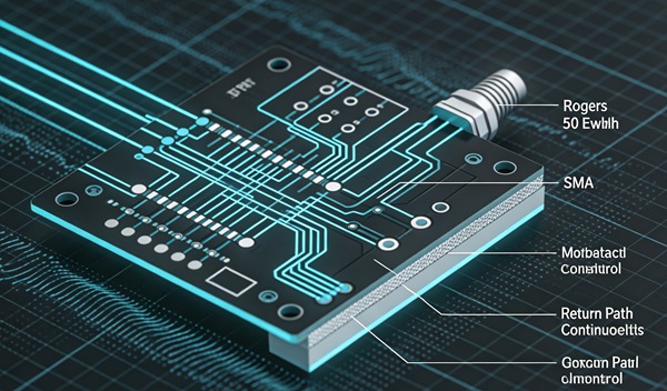
Two primary material properties govern RF signal behavior: the Dielectric Constant (Dk, or relative permittivity) and the Dissipation Factor (Df, or loss tangent).
The Dielectric Constant (Dk) determines the velocity of signal propagation through the medium and the capacitive coupling between conductors. In RF design, consistency across the spectrum is just as critical as the absolute value. Variations in Dk across a single board, or between different manufacturing batches, can cause localized impedance mismatches and phase shifts, destroying the performance of precisely tuned RF filters and antenna matching networks. Rogers materials, such as the widely adopted RO4000® series and the PTFE-based RT/duroid® series, are engineered for tightly controlled Dk tolerances across exceptionally broad frequency spectrums and varying temperature ranges.
The Dissipation Factor (Df) dictates the amount of electromagnetic energy that is actively absorbed by the dielectric material and permanently dissipated as thermal energy (heat). This phenomenon is known as dielectric loss. At microwave frequencies, dielectric loss becomes a dominant factor in signal attenuation, severely limiting the transmission distance. Standard FR-4 typically exhibits a Df of around 0.02, which is unacceptably high and results in catastrophic signal degradation for high-frequency applications. In stark contrast, advanced Rogers laminates boast Df values as astoundingly low as 0.0009.
Furthermore, the choice of laminate fundamentally affects conductor loss. At high frequencies, the “skin effect” forces the alternating current to flow almost exclusively along the extreme outer microscopic surface of the copper trace. If the copper foil surface bonded to the dielectric is rough—which is standard practice to promote mechanical adhesion in FR-4—the signal is forced to traverse the microscopic peaks and valleys. This drastically increases the effective path length and, consequently, the conductor losses. Rogers materials utilize specialized manufacturing treatments that allow for exceptionally smooth copper foils (such as Rolled Annealed or Reverse Treated copper profiles) while maintaining structural adhesion, thereby neutralizing skin effect losses.

Mastering Impedance Matching in RF Circuits
Impedance matching is the absolute cornerstone of RF engineering. Dictated by the maximum power transfer theorem, to deliver the maximum amount of power from a source (such as an RF amplifier) to a load (such as an antenna), the source impedance must exactly equal the complex conjugate of the load impedance. In standard telecommunications and RF systems, this characteristic impedance is almost universally standardized at 50 ohms.
If the characteristic impedance of the PCB transmission line deviates from this 50-ohm standard—due to incorrect trace width, localized dielectric thickness variations, or abrupt geometric changes—a portion of the RF signal is reflected backward toward the source rather than being transmitted to the load. This phenomenon is mathematically quantified by the Voltage Standing Wave Ratio (VSWR) or Return Loss (S11). High signal reflections not only starve the load component of necessary power but can also create intense standing waves along the transmission line that can permanently damage sensitive power amplifiers and degrade receiver noise figures. Learn more about Biocompatible PCBs: Advanced Materials for Implantable Medical Devices.
Achieving precise impedance matching with Rogers materials involves selecting the most appropriate transmission line topology for the specific application:
- Microstrip: This is the most common and easily manufacturable topology, consisting of a carefully sized trace routed on the top or bottom outer layer with a solid, continuous ground plane situated on the adjacent internal layer directly beneath it. It offers ease of fabrication, debugging, and component placement. However, because the electromagnetic field travels partially through the dielectric substrate and partially through the surrounding air, it experiences an “effective” Dk, making exact analytical calculations slightly more complex and increasing the propensity for unwanted electromagnetic radiation at higher millimeter-wave frequencies.
- Stripline: This topology involves a copper trace sandwiched symmetrically between two solid ground planes and encapsulated entirely within the dielectric material. Stripline offers superior Electromagnetic Interference (EMI) shielding and non-dispersive signal propagation since the electromagnetic wave travels exclusively through a homogeneous dielectric medium. The engineering tradeoff is the requirement for stricter manufacturing tolerances, increased overall board thickness, and the absolute necessity of utilizing blind vias to transition signals to surface components.
- Coplanar Waveguide (CPW): CPW features a central signal trace flanked by wide ground planes on the exact same layer, separated by a meticulously calculated gap. It is often backed by a lower ground plane to form Grounded CPW (GCPW). CPW provides unparalleled isolation, significantly reduced dispersion, and allows for much easier mounting of surface-mount RF components without requiring highly inductive vias to reach a lower ground reference plane.
Dielectric Loss Control: Optimizing Beyond the Material Data Sheet
While proactively selecting a low-loss Rogers laminate like RO4350B or RO3003 is the mandatory first step, actualizing low dielectric loss in a physical printed circuit board layout requires rigorous, holistic engineering. The cumulative insertion loss (S21) of an RF trace is the mathematical sum of dielectric loss, conductor loss, radiation loss, and leakage loss. Learn more about Flex PCB Stiffeners: Choosing Between FR4, Polyimide, and Stainless Steel.
To minimize overall loss, RF engineers must meticulously optimize the trace geometry in close conjunction with the PCB material stackup. A thicker dielectric core allows for a geometrically wider copper trace to maintain the required 50-ohm characteristic impedance. A wider trace significantly reduces the conductor loss and skin effect resistance. However, a thicker dielectric increases the overall vertical profile of the RF fields, potentially leading to the excitation of unwanted spurious substrate modes or increased radiation if not aggressively constrained by via fencing and grounding structures. Learn more about AXI X-Ray Inspection: Detecting PTH Fill and Barrel Cracking Defects.
Moisture absorption is often the silent, unpredictable killer of RF performance in harsh environments. Pure water possesses a highly volatile Dk of approximately 80 and a massive dissipation factor. If a PCB substrate absorbs ambient humidity from the atmosphere, its effective Dk and Df will spike dramatically, instantly ruining carefully calculated impedance matching and heavily attenuating the propagating signal. While standard materials behave like sponges, absorbing significant moisture, PTFE-based Rogers materials (like the RT/duroid series) are virtually non-hygroscopic, ensuring incredibly stable environmental performance across decades of deployment.
Furthermore, designers must heavily scrutinize the impact of solder mask. Standard Liquid Photoimageable (LPI) solder mask typically exhibits a high Df and an unpredictable Dk that can vary by manufacturer and application thickness. For critical RF transmission lines, it is standard industry practice to explicitly define a solder mask opening (a solder mask keep-out region) strictly over the RF traces to prevent the coating from altering the calculated effective dielectric constant and introducing parasitic dielectric loss.
Advanced RF Routing and PCB Layout Strategies
High-frequency RF routing requires a complete paradigm shift away from traditional digital layout practices. Through-hole vias, which are completely benign in low-speed digital designs, instantly become highly reactive inductive and capacitive discontinuities at RF frequencies. When a via must transition an RF signal between internal layers, the transition impedance must be meticulously modeled in 3D. This almost always requires “via stitching” (placing specific ground vias coaxially surrounding the central signal via) to provide an immediate, controlled return path for the ground currents and maintain the 50-ohm characteristic of the transition.
Geometric corners and trace bends must be explicitly managed. A standard, sharp 90-degree corner adds excess localized capacitance, causing an immediate impedance drop and subsequent signal reflection. High-frequency RF traces must exclusively utilize optimally calculated mitered 45-degree bends or, preferably, sweeping radial curves with a bend radius of at least three times the trace width. Learn more about Medical PCB Assembly: ISO 13485 Compliance & Traceability.
Additionally, ensuring proper electromagnetic isolation between parallel RF chains (such as transmit and receive paths) is vital to prevent catastrophic crosstalk and oscillation. This isolation is achieved through adequate physical spacing (the standard digital 3W rule is wholly insufficient for RF; 5W or physical shielding is strictly preferred), orthogonal routing on adjacent inner layers, and the highly strategic placement of copper ground pours populated with tightly spaced via fences to aggressively block electromagnetic surface wave propagation laterally through the dielectric substrate.
How to Design an RF PCB Using Rogers Materials (Step-by-Step Guide)
Follow these engineering rules.
- Select the Appropriate Rogers Material
Evaluate the target operating frequency, environmental operating conditions, required thermal conductivity, and project budget. For sub-6 GHz applications, hydrocarbon ceramic-filled laminates like Rogers RO4350B offer an excellent, cost-effective balance of low loss and standard FR-4-like fabrication processability. For demanding millimeter-wave (mmWave) applications operating above 30 GHz (such as automotive radar), PTFE-based materials such as RO3003 or RT/duroid 5880 are strictly mandatory due to their ultra-low dissipation factor (Df) and minimal frequency dispersion.
- Define the Stackup and Calculate Impedance
Utilize an advanced 2D or 3D electromagnetic field solver to determine the exact trace widths, gaps, and clearances required to precisely achieve a 50-ohm characteristic impedance. Never rely on simplified, free online impedance calculators for critical RF designs. Input the exact manufacturer-specified core thickness, prepreg properties, finished copper weight, and expected copper surface roughness profile. If utilizing a hybrid stackup (using Rogers for outer RF layers and FR-4 for inner digital and power layers), coordinate with your PCB fabrication house to ensure they can manage the different pressing cycles, curing temperatures, and dimensional stabilities of the dissimilar materials.
- Route the RF Transmission Lines
Begin your layout by routing the most critical, highest-frequency RF signal paths first. Keep these traces as short and physically direct as absolutely possible to minimize total insertion loss. Completely avoid sharp corners by implementing calculated miters or wide radial curves. Ensure that no other traces, power planes, split plane gaps, or high-speed digital signals run parallel or cross perpendicularly within the immediate electromagnetic field boundary of the sensitive RF trace.
- Implement Grounding and Shielding Strategies
Establish a solid, unbroken, and continuous ground plane directly adjacent to the RF signal layer. Implement dense via fences (a continuous row of grounded vias) along the entire edges of RF microstrip traces or coplanar waveguides to physically suppress unwanted substrate modes and dramatically improve inter-channel isolation. The center-to-center spacing between these shielding ground vias must be calculated to be less than one-twentieth (1/20) of the wavelength of the highest expected operating frequency in the system.
- Verify and Simulate the Design
Export the critical RF routing layouts, including all adjacent ground structures, to a comprehensive 3D electromagnetic (EM) simulator suite (such as Ansys HFSS or Keysight ADS). Thoroughly simulate the S-parameters—specifically focusing on Insertion Loss (S21) and Return Loss (S11)—of the layer transitions, via structures, and long trace runs. Iteratively refine the layout, adjusting via pad sizes, internal layer anti-pad clearances, and trace geometries until the simulated performance comfortably meets the stringent design specifications across the entire operating frequency bandwidth.
Frequently Asked Questions (FAQ)
While it is technically possible to use standard FR-4 for very short trace runs at 2.4 GHz, the inherently high Dissipation Factor (Df) of FR-4 will result in significant signal attenuation (power loss) as the trace lengthens. This directly reduces the effective wireless range and drastically shortens the battery life of the mobile device. Additionally, the unpredictable and widely varying Dielectric Constant (Dk) of FR-4 across batches makes precise 50-ohm impedance matching exceptionally difficult, leading to internal signal reflections and further power degradation. Rogers materials provide the strict low loss and Dk stability required for optimal, repeatable RF performance.
A hybrid PCB stackup strategically combines expensive, high-performance Rogers laminates exclusively for the critical RF layers (usually the top or bottom outer microstrip layers) with standard, highly cost-effective FR-4 materials for the internal routing of low-speed digital signals, power distribution networks, and ground planes. This intelligent composite approach drastically reduces the overall manufacturing cost compared to building a pure multi-layer Rogers board, while simultaneously delivering superior RF performance exactly and only where it is electromagnetically needed.
At high RF and microwave frequencies, the “skin effect” causes electrical current to travel exclusively along the very outer perimeter (the skin) of the copper trace. If the copper foil profile is rough (a technique often used to help it mechanically adhere to the epoxy dielectric), the high-frequency signal is forced to travel up and down the microscopic peaks and valleys. This effectively increases the physical path length and the surface electrical resistance, resulting in significantly higher conductor losses. High-end Rogers materials often utilize specialized low-profile or reverse-treated copper foils to drastically minimize this detrimental effect.
Generally, it is strongly advised not to cover critical, high-frequency RF transmission lines with standard liquid photoimageable (LPI) solder mask. Solder mask materials possess relatively high and notoriously poorly controlled Dk and Df values that are rarely documented accurately for high frequencies. Applying a layer of solder mask directly over a carefully calculated microstrip line will unpredictably alter its effective dielectric constant, shifting the characteristic impedance away from 50 ohms and simultaneously introducing significant additional parasitic dielectric loss. Instead, engineers specify solder mask keep-out windows strictly over these sensitive traces.
Standard microstrip is significantly simpler to design, model, and manufacture, making it highly ideal for lower RF frequencies and straightforward, direct point-to-point surface routing. However, GCPW offers drastically superior channel isolation, considerably lower radiation loss, and significantly less frequency dispersion at extremely high operational frequencies (e.g., mmWave radar applications). Crucially, GCPW also provides highly convenient and immediate ground access directly on the top routing layer. This is immensely beneficial for mounting surface-mount RF components and shunt elements without introducing the highly detrimental parasitic inductance inherently associated with through-hole vias.