High-frequency PCBs are designed to carry radio frequency (RF) and microwave signals with minimal signal loss and distortion. As wireless communication technologies continue to advance, high-frequency circuit boards have become essential in industries such as telecommunications, aerospace, automotive radar, satellite communications, medical electronics, and industrial automation.
Unlike standard FR4 boards, high-frequency PCBs require specialized materials, precise impedance control, and advanced manufacturing processes to maintain signal integrity at frequencies ranging from hundreds of megahertz to tens of gigahertz.
Understanding the design and manufacturing requirements of high-frequency PCBs is critical for achieving reliable performance in modern electronic systems.
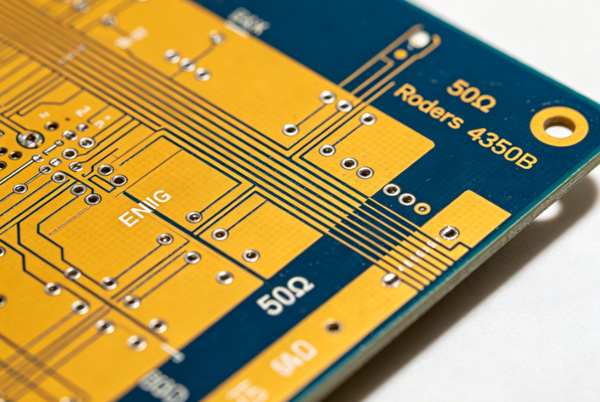
Table of Contents
What Is a High-Frequency PCB?
A high-frequency PCB is a circuit board specifically engineered to support the transmission of high-speed RF and microwave signals.
These boards are commonly used when operating frequencies exceed 500 MHz and become increasingly critical in applications above 1 GHz.
Compared with conventional PCBs, high-frequency boards focus heavily on:
- Signal integrity
- Low dielectric loss
- Controlled impedance
- Stable electrical performance
- Electromagnetic compatibility
As signal frequencies increase, even small variations in PCB materials or manufacturing tolerances can significantly affect circuit performance.
Why Standard FR4 Is Not Always Suitable
FR4 remains the most common PCB substrate for general electronics, but its electrical properties may become limiting in RF and microwave applications.
Common challenges include:
- Higher dielectric loss
- Increased signal attenuation
- Impedance variation
- Poor phase stability
- Reduced performance at high frequencies
For low-frequency digital circuits, these limitations may be negligible. However, for radar systems, RF amplifiers, antennas, and high-speed communication devices, specialized high-frequency materials are often required.
Related article: Multilayer PCB Manufacturing
High-Frequency PCB Materials
Material selection is one of the most important decisions in RF PCB design.
Rogers Materials
Rogers laminates are among the most widely used materials for high-frequency applications.
Advantages include:
- Low dielectric loss
- Stable dielectric constant
- Excellent thermal performance
- Consistent electrical properties
Common Rogers material families include:
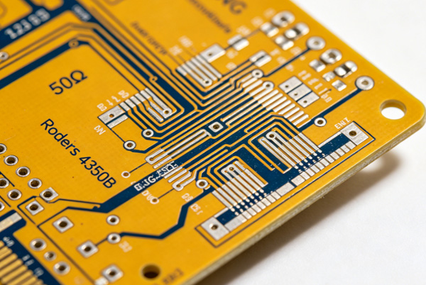
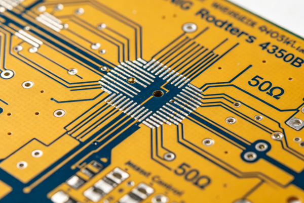
- RO4003C
- RO4350B
- RO4835
- RT/duroid Series
These materials are frequently used in communication infrastructure and radar systems.
PTFE-Based Materials
PTFE (Polytetrafluoroethylene) materials offer excellent RF performance.
Benefits include:
- Extremely low loss tangent
- Stable electrical characteristics
- Excellent microwave performance
PTFE substrates are commonly found in:
- Aerospace systems
- Satellite communication equipment
- Military electronics
- Advanced radar applications
Hybrid PCB Structures
Many designs combine FR4 and high-frequency materials within the same stackup.
This approach helps balance:
- Manufacturing cost
- Electrical performance
- Mechanical strength
Hybrid constructions are widely used in automotive radar and wireless communication products.
Key Electrical Properties
Dielectric Constant (Dk)
The dielectric constant affects signal propagation speed and impedance calculations.
Lower and more stable Dk values generally improve signal predictability.
Typical high-frequency materials provide tighter Dk control than standard FR4.
Dissipation Factor (Df)
The dissipation factor measures signal energy loss within the substrate.
Lower Df values help reduce:
- Insertion loss
- Signal degradation
- Heat generation
This becomes increasingly important as frequencies rise.
Thermal Stability
High-frequency systems often operate continuously under demanding environmental conditions.
Thermally stable materials help maintain:
- Consistent impedance
- Reliable signal transmission
- Long-term performance
High-Frequency PCB Stackup Design
Stackup design directly affects signal quality.
A properly designed stackup helps control:
- Impedance
- Crosstalk
- Electromagnetic interference
- Return current paths
Common stackup practices include:
- Dedicated ground planes
- Symmetrical layer structures
- Controlled dielectric spacing
- Short signal paths
High-layer-count RF boards often combine signal layers with continuous reference planes to maintain signal integrity.
Related reading: PCB Stackup Design Guide
Controlled Impedance Requirements
Controlled impedance is a fundamental requirement for most high-frequency circuits.
Common impedance targets include:
- 50 Ohm single-ended traces
- 75 Ohm RF systems
- 90 Ohm differential pairs
- 100 Ohm differential pairs
Maintaining impedance within specified tolerances requires precise control of:
- Trace width
- Copper thickness
- Dielectric thickness
- Material properties
Manufacturers typically verify impedance through simulation and testing during production.
Signal Integrity Considerations
As frequency increases, PCB layout becomes increasingly important.
Designers must pay attention to:
Trace Length Control
Long signal paths increase attenuation and introduce timing issues.
Shorter routing generally improves signal quality.
Grounding Strategy
Continuous ground planes provide stable return paths and reduce electromagnetic interference.
Ground interruptions can negatively impact RF performance.
Via Design
Poorly designed vias can introduce impedance discontinuities and signal reflections.
Techniques such as back-drilling and optimized via structures may be used for critical RF paths.
Crosstalk Reduction
Adequate spacing between high-frequency traces helps reduce unwanted signal coupling.
Proper layer assignment and shielding techniques further improve performance.
Surface Finish Selection
Surface finish affects both assembly quality and RF performance.
Common options include:
ENIG
Widely used for:
- Fine-pitch components
- RF modules
- High-density designs
Benefits include excellent flatness and reliable solderability.
Immersion Silver
Popular in RF applications because of its favorable conductivity characteristics.
Advantages include:
- Low contact resistance
- Good RF performance
- Excellent solderability
Surface finish selection should be evaluated based on both manufacturing requirements and electrical performance goals.
Manufacturing Challenges of High-Frequency PCBs
Producing high-frequency boards requires tighter process control than conventional PCBs.
Key challenges include:
Material Handling
Specialized laminates often require different drilling and lamination parameters.
Dimensional Accuracy
Small variations in trace geometry can affect impedance and RF performance.
Registration Control
Multilayer RF boards demand precise layer alignment.
Impedance Verification
Manufacturers must ensure finished boards meet impedance specifications through process control and testing.
These requirements make experience and manufacturing capability particularly important when selecting a supplier.
Related article: What Quality Standards Indicate a Reliable PCB Manufacturer?
Common Applications of High-Frequency PCBs
5G Infrastructure
High-frequency PCBs are widely used in:
- Base stations
- Small cells
- Network equipment
Automotive Radar
Modern vehicles increasingly rely on radar systems operating at frequencies such as 24 GHz and 77 GHz.
Related application: Autonomous Delivery Vehicle PCB
Satellite Communications
Satellite systems require low-loss RF transmission and highly stable electrical performance.
Aerospace and Defense
Mission-critical communication and radar systems depend heavily on high-frequency PCB technology.
Medical Equipment
Advanced diagnostic and imaging systems often incorporate RF circuits and microwave technologies.
Quality Standards for High-Frequency PCB Manufacturing
Reliable high-frequency PCB production typically follows:
- IPC-A-600
- IPC-6012
- ISO 9001
- UL-recognized materials
- RoHS compliance
Additional verification may include:
- Impedance testing
- Cross-section analysis
- Material certification review
- Electrical testing
- AOI inspection
Because RF performance is highly sensitive to manufacturing variation, process consistency is essential.
Choosing a High-Frequency PCB Manufacturer
When evaluating suppliers, consider:
- Experience with RF materials
- Controlled impedance capability
- Hybrid stackup expertise
- Engineering support
- Material sourcing capability
- Quality certifications
- Testing procedures
Manufacturers that regularly produce RF and microwave boards are typically better equipped to manage the unique challenges associated with high-frequency designs.
Conclusion
High-frequency PCBs play a critical role in modern communication, radar, aerospace, automotive, and industrial systems.
Successful RF PCB projects depend on the combination of proper material selection, controlled impedance design, optimized stackup structures, and precise manufacturing processes.
Working with an experienced high-frequency PCB manufacturer helps ensure stable electrical performance, reduced signal loss, and reliable operation across demanding applications.
FAQ
A: Many engineers consider frequencies above 500 MHz to be high frequency, although specialized RF materials are often required above 1 GHz.
A: Rogers RO4350B and RO4003C are among the most widely used materials for RF and microwave applications.
A: Controlled impedance helps maintain signal integrity, reduce reflections, and ensure predictable electrical performance.
A: FR4 can support some lower-frequency RF applications, but specialized materials generally provide better performance at higher frequencies.
A: Telecommunications, aerospace, defense, automotive radar, satellite communications, industrial automation, and medical electronics all rely on high-frequency PCB technology.