Smart Home PCB Manufacturing
& Assembly Services
Scalable, High-Reliability PCB Solutions for Home Automation, Smart Appliances, Security and Connected Lighting Systems.
Why Choose Us for Smart Home PCB
We empower the connected home ecosystem by delivering high-volume, cost-efficient PCBs optimized for the latest wireless standards and user-interface technologies.
Wireless Connectivity Support
Expert layout and matching for specialized home protocols including Matter, Zigbee, Thread, Wi-Fi 6, and Bluetooth Mesh.
Advanced HMI Mastery
Precision HDI manufacturing for high-resolution touch panels, LCD drivers and smart display interfaces for connected panels.
Cost-Optimized Scaling
Strategic Design for Manufacturing (DFM) focused on reducing unit costs for high-volume consumer smart home devices.
Rapid Turnaround
Support for fast iterative prototyping to help your product team move quickly from concept to a consumer-ready launch.
Full Turnkey Assembly
Complete SMT and through-hole assembly services, including component sourcing for complex IoT multi-sensor modules.
IoT-Specific Engineering
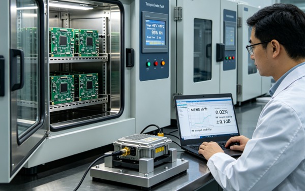
Dedicated IoT engineers provide RF antenna design, power management optimization and high-speed data integrity analysis.
Agile Engineering for the Connected Home
Our smart home engineering specialists partner with your team to navigate the complexities of IoT hardware — optimizing energy efficiency, wireless performance and component density for retail success.
Designing hardware compatible with the latest unified smart home connectivity standards.
Strategic RF layout to ensure maximum range and stability for home automation devices.
Optimizing PCB layouts for battery-powered smart sensors requiring multi-year operational life.
Securing long-term stability in high-volume production through verified global supply chains.
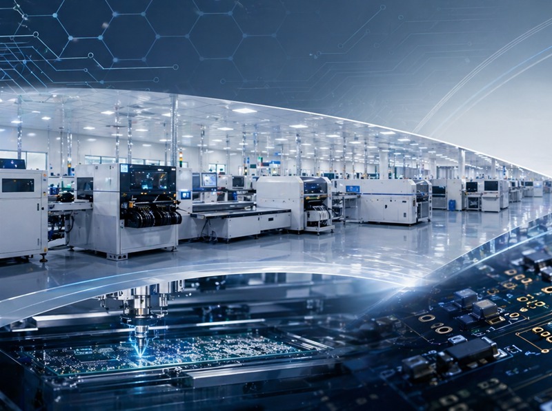
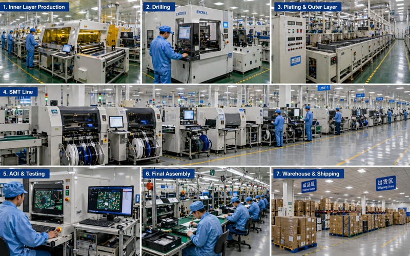
Smart Home PCB Manufacturing Capabilities
TopfastPCB delivers scalable PCB solutions for the entire smart home landscape, from central automation hubs to low-power peripheral sensors and smart appliances.
Smart Display HDI
High-density multi-layer PCBs for smart touch-screens, HMI control panels and intelligent dashboards.
Automation Hubs
Reliable motherboard solutions for smart gateways, routers and central home automation control units.
Smart Sensor Boards
Ultra-compact PCBs for door sensors, leak detectors, thermostats and connected environmental monitoring.
High-Speed Execution Workflow
Rapid engineering review and technical viability for volume production.
Multilayer fabrication with integrated wireless layer testing.
High-speed SMT lines for rapid mass assembly of IoT modules.
100% automated testing ensuring seamless home network operation.
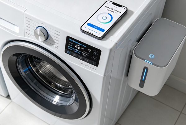
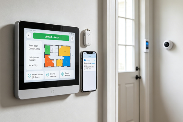
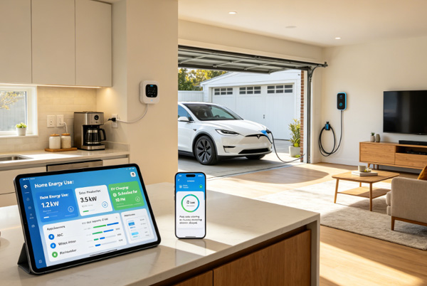
Smart Home Applications
TopfastPCB powers the world's most innovative connected home brands, providing scalable reliability across every smart appliance and automation category.


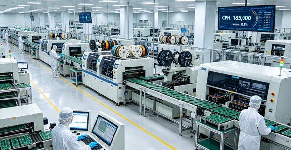
Mass Production Ecosystem
Our world-class manufacturing facility is optimized for high-volume IoT production, featuring high-speed automated SMT lines and state-of-the-art RF testing labs.
Chosen by the World's Leading IoT Brands
Innovative smart home brands and global ecosystem leaders rely on TopfastPCB for their connected hardware infrastructure.


Smart Home FAQ
Common questions about Smart Home & IoT PCB development, scaling and standards.
Ask a Specialist →Yes. Our engineering team is fully experienced in designing for the Matter protocol via Thread and Wi-Fi 6, ensuring your hardware meets the unified industry standard for connected home devices.
We specialized in RF (Radio Frequency) layout design, including antenna matching and trace impedance control, to maximize signal strength and reduce interference in congested home wireless environments.
Absolutely. Our facility is designed for scale, with a monthly capacity of over 1.5 million units, making us an ideal partner for global consumer smart home brands during large-scale product rollouts.
Yes. Cost efficiency is critical in the smart home market. Our Engineers provide extensive Design for Manufacturing (DFM) reviews to optimize board size, material selection and fabrication complexity to lower your overall cost-per-unit.