Consumer Electronics PCB
& Assembly Services
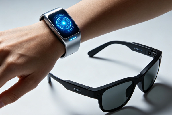
Scalable, High-Performance PCB Solutions for Smartphones, Wearables, Smart Home Devices and Personal Computing.
Why Choose Us for Consumer Electronics PCB
From high-speed processing to ultra-compact designs, we provide the scalability and advanced technology required to win in the fast-paced consumer market.
Advanced HDI Capability
Expertise in any-layer HDI and microvia technology, enabling the extreme miniaturization required for modern smartphones and wearables.
Ultra-Thin & High-Density
Manufacturing ultra-thin substrates (down to 0.2mm) with 2.5 mil trace/space for compact, multi-layer consumer designs.
Cost Optimization
Design for Manufacturing (DFM) support focused on reducing production costs while maintaining high quality for volume markets.
Rapid GTM Support
Speed-to-market is critical. We offer lightning-fast prototype services to accelerate your iterative product development cycles.
Scalable Mass Production
From initial proof-of-concept to millions of units, our facility is equipped to handle your entire product lifecycle scaling.
Signal Integrity Mastery
Specialized high-speed digital design support to ensure flawless performance in data-heavy devices and wireless communications.

Engineering Agility for High-Growth Consumer Tech
Our consumer electronics engineering team partners with you to bridge the gap between design and volume production — maximizing PCB reliability, component density, and cost-efficiency.
Optimizing layouts for 0.4mm pitch BGA and ultra-fine trace/space requirements.
Antenna design and RF layout support for Wi-Fi 6, 5G, and Bluetooth Low Energy (BLE).
Designing for unconventional shapes using hybrid rigid-flex and ultra-thin substrates.
Value engineering to reduce BOM costs and fabrication complexity for high-volume consumer goods.
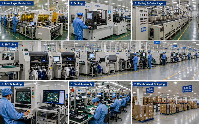
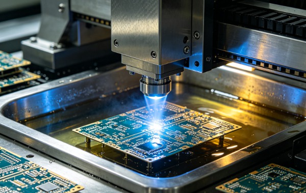
Consumer PCB Manufacturing Capabilities
TopfastPCB delivers high-precision PCB solutions for the global consumer electronics market, from ultra-thin smartphone boards to complex multi-layered IoT device circuitry.
Any-Layer HDI
The most advanced interconnect technology for complex smartphones and tablets with high pin-count BGAs.
Rigid-Flex Fusion
Hybrid technology combining stability and flexibility, perfect for foldable devices and ergonomic wearables.
Ultra-Thin HDI
Substrates as thin as 0.2mm for ultra-slim consumer laptops and high-performance handheld devices.
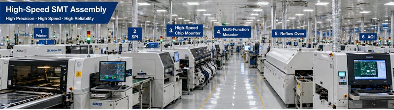
High-Speed Production Workflow
Instant engineering review and technical viability check.
Agile manufacturing for both prototypes and mass production.
High-speed SMT lines for rapid component placement and soldering.
Full suite of automated testing for 100% functional reliability.
Consumer Electronics Applications
TopfastPCB powers the world's most innovative consumer technology brands, providing scales of reliability across diverse product categories.


High-Capacity Manufacturing Hub
Our world-class manufacturing facility is optimized for high-volume consumer production, featuring state-of-the-art SMT lines, advanced HDI plating, and precision testing automation.
Trusted by Consumer Tech Leaders Worldwide
Leading smartphone brands, IoT innovators and wearable technology companies rely on TopfastPCB for their global product launches.


Consumer PCB FAQ
Common questions about high-volume and rapid-prototype consumer electronics PCB production.
Ask a Specialist →We offer expedited prototype services with turnaround times as low as 24-48 hours from Gerber file approval, helping you accelerate your iterative product development and reduce time-to-market.
We support up to Any-Layer HDI (ELIC), stacked and staggered microvias, and fine-pitch BGA (0.4mm and below) to enable the maximum component density required for complex high-end mobile devices.
Our engineering team provides comprehensive DFM support to optimize board layouts, panel utilization, and manufacturing processes, reducing material waste and overall production costs for high-volume orders.
Yes. We provide complete turnkey PCB Assembly (PCBA) services, including component sourcing, pick-and-place, reflow soldering, and functional testing, letting you focus on product design and marketing.