IoT PCB Manufacturing
& Assembly Services
Ultra-Compact, Low-Power PCB Solutions for Industrial IoT (IIoT), Asset Tracking, Smart Cities and Connected Sensors.
Why Choose Us for IoT PCB
We bridge the gap between digital data and physical sensors by delivering the most compact, battery-efficient, and wireless-optimized PCBs for the global IoT market.
Multi-Protocol RF Expertise
Specialized layout for long-range and cellular IoT, including LoRaWAN, NB-IoT, Sigfox, LTE-M and 5G NR.
Micro-Miniaturization
Advanced HDI capabilities with fine-pitch traces and blind/buried vias to fit complex electronics into ultra-small IoT form factors.
Ultra-Low Power Design
Engineering support to minimize parasitic capacitance and leakage, extending the battery life of remote wireless nodes.
Rapid Prototyping
Iterative design support for R&D teams, providing quick-turn prototypes to validate IoT hardware before mass deployment.
Environmental Ruggedness
Selection of conformal coatings and moisture-resistant substrates for IoT devices operating in harsh outdoor or industrial settings.
Full SMT Assembly
Precision component placement for ultra-small 0201 packages and dual-sided assembly for complex IoT sensor modules.

Intelligent Engineering for a Connected World
Our dedicated IoT engineering team helps you solve the toughest connectivity and power challenges — ensuring your smart devices perform flawlessly across diverse network environments.
Simulation and matching for integrated antennas to maximize range and connection stability.
Strategic layout to minimize current spikes and maximize operational life for battery-powered nodes.
Optimizing dense HDI layouts to ensure high yield in high-volume micro-IoT production.
Design guidance for ensuring pre-compliance with LoRa, NB-IoT and Sigfox regional standards.
IoT PCB Manufacturing Capabilities
TopfastPCB provides specialized fabrication for the global internet of things landscape, from industrial sensor arrays to ultra-small consumer wearable nodes.
Rigid-Flex Nodes
Optimized rigid-flex solutions for non-standard sensor shapes and high-reliability wearable IoT devices.
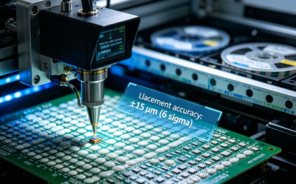
HDI Miniaturization
Stacked microvia technology allowing complex 5G and cellular IoT designs to fit in thumb-sized enclosures.
Industrial IIoT
Heavy-duty, high-Tg PCBs for industrial automation sensors and rugged outdoor smart city infrastructure.
Integrated IoT Workflow
Rapid engineering review focusing on RF performance and power efficiency.
Dense multilayer fabrication with tight impedance control for RF integrity.
High-speed SMT assembly optimized for micro-components and complex IoT modules.
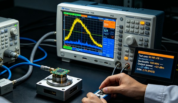
Full functionality validation including wireless signal strength and sleep-mode testing.
IoT Application Ecosystem
TopfastPCB powers the global massive IoT expansion, providing reliable connectivity across diverse industrial and consumer sectors.


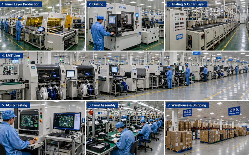
Precision IoT Manufacturing Center
Our world-class facility is optimized for the micro-scale and wireless complexity of IoT hardware, featuring specialized SMT for fine-pitch components and integrated RF verification.
Trusted by IoT Innovators Worldwide
Leading IoT product companies, smart city labs and industrial automation firms rely on TopfastPCB for their global connected hardware rollouts.


IoT PCB FAQ
Common questions about IoT and wireless sensor PCB development and manufacturing.
Ask a Specialist →We provide engineering reviews focusing on substrate material choice and high-precision routing to minimize trace capacitance and leakage current, which are critical for the multi-year battery life of remote smart sensors.
Yes. Our RF experts offer specialized guidance on antenna matching, ground plane optimization and layout impedance control for NB-IoT, LoRa and Wi-Fi antennas to ensure maximum communication range.
We provide full conformal coating services, potting-ready board designs and moisture-resistant surface finishes (like ENEPIG) to ensure your IoT hardware survives extreme humidity and chemical exposure in outdoor or industrial settings.
We leverage ultra-thin core substrates and elite HDI technology (any-layer microvias) with 2.5 mil trace/space capability to fit high-speed cellular components and sensing circuitry onto the smallest wearable form factors.