Semiconductor PCB Manufacturing
& Assembly Services
Ultra-High Layer Count, Precision Impedance and Advanced Thermal Solutions for ATE Load Boards, Burn-in Boards and Probe Card Interfaces.
Why Choose Us for Semiconductor PCB
We deliver the extreme precision and material performance required for complex integrated circuit testing, where signal integrity and thermal reliability are non-negotiable.
Ultra-High Layer Density
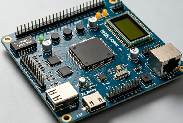
Expert manufacturing of high-layer count boards (up to 50+ layers) with complex blind, buried and stacked microvia architectures.
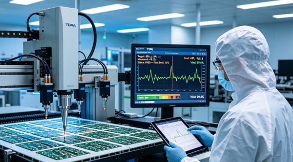
Precision Impedance Control
Advanced TDR testing ensuring tight impedance tolerances (±5% down to ±2% upon request) for ultra-high speed signal paths.
Advanced Thermal Materials
Working with specialized substrates (Rogers, Megtron 6/7, Tachyon 100G) to handle high-power dissipation in burn-in environments.
Micro-Pitch BGA Assembly
SMT placement capability for 0.3mm – 0.4mm pitch BGA and CSP components, essential for high-pin count semiconductor interfaces.
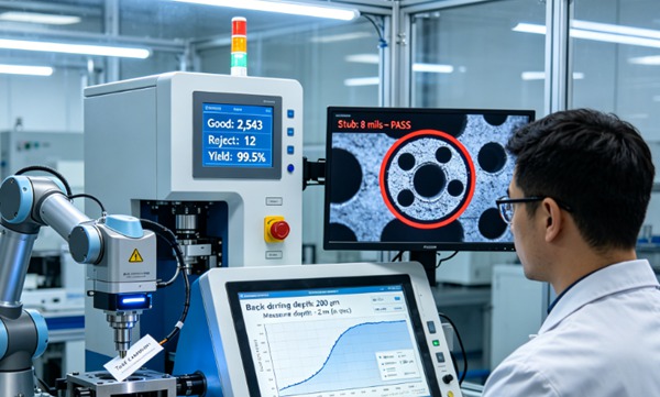
Back-Drilling Mastery
In-house precision back-drilling to eliminate signal stubs and minimize reflection in high-frequency ATE applications.
Evaluation to Production
Seamless transition from custom evaluation boards (EVB) to mass burn-in board (BIB) and load board production.
Elite Engineering for High-Speed Chip Testing
Our semiconductor engineering specialists partner with IC design and test teams to optimize the critical interface between the chip and the automated test equipment (ATE) — maximizing signal integrity and yield.
Strategic signal routing and isolation to protect against cross-talk and data-link degradation.
Hybrid material selection (e.g. FR4 + High-Speed Rogers) to balance cost and ultra-low loss performance.
Advanced heat dissipation analysis for high-power AI and server chips under test conditions.
Rigorous design reviews ensuring manufacturability of the industry's most dense board architectures.
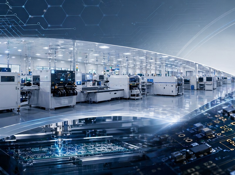
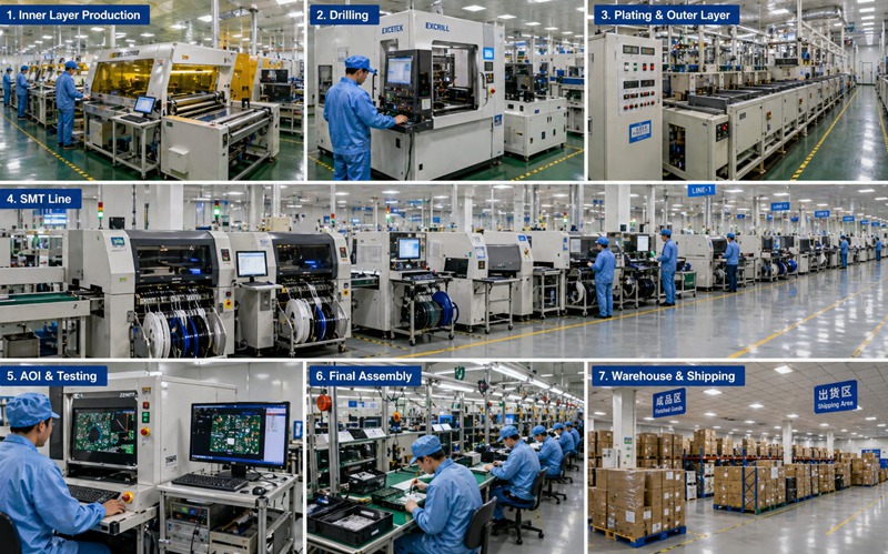
Semiconductor PCB Manufacturing Capabilities
TopfastPCB provides the extreme specification hardware required for the semiconductor lifecycle, from initial silicon evaluation to massive burn-in and system-level testing.
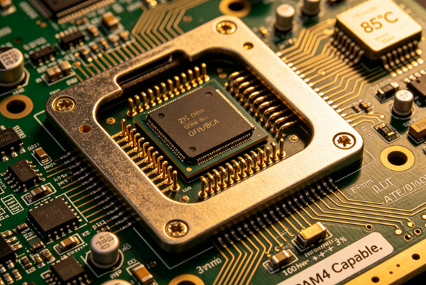
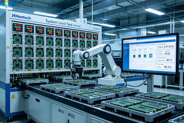
ATE Load Boards
Multilayer, precision-impedance boards connecting IC samples to high-speed automated test equipment.
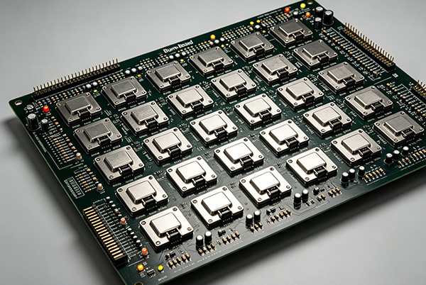
Burn-in Boards (BIB)
Reliable, high-temperature boards designed for long-duration screening and thermal stress testing.
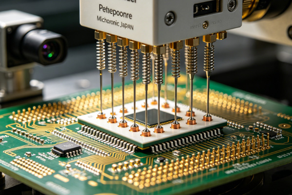
Probe Card PCB
Ultra-flat interface PCBs for probe card assemblies, enabling direct wafer-level semiconductor testing.
Semiconductor Grade Workflow
Expert review for complex layer counts and exotic material stack-ups.
Integrated back-drilling and TDR impedance control for sub-path integrity.
Elite assembly for fine-pitch BGA and high-pin count test connectors.
Full-spectrum validation ensuring zero signal link loss for IC testing.
Semiconductor Lifecycle Support
TopfastPCB powers the world's leading chipmakers, providing critical interface hardware across every phase of the semiconductor test cycle.
Precision IC Test Innovation Center
Our advanced manufacturing facility is optimized for the extreme layer counts and signal performance required for semiconductor testing, featuring elite TDR and thermal verification.
Chosen by the World's Leading Chipmakers
Innovative IC design houses, global IDMs and ATE equipment leaders rely on TopfastPCB for their most demanding test hardware.


Semiconductor PCB FAQ
Common questions about IC test board manufacturing, impedance control and ATE standards.
Ask a Specialist →We leverage industry-leading fabrication technology to produce boards with 50+ layers. This capability is essential for complex semiconductor load boards and probe cards that require massive parallel routing and dedicated power planes.
We provide standard impedance control at ±5%. For ultra-critical high-frequency paths in ATE and high-speed IC evaluation, we can achieve precision tolerances as tight as ±2% using verified material stack-ups and advanced TDR testing.
Yes. We use precision laser and mechanical back-drilling to remove redundant plating stubs. This is a critical requirement for ATE load boards to ensure clean signals and minimize reflection at frequencies above 10GHz.
For high-power AI and server chips, we design boards with heavy copper layers (up to 12oz) and metal core inserts or copper-coin technology to manage the extreme thermal loads produced during long-duration burn-in cycles.