
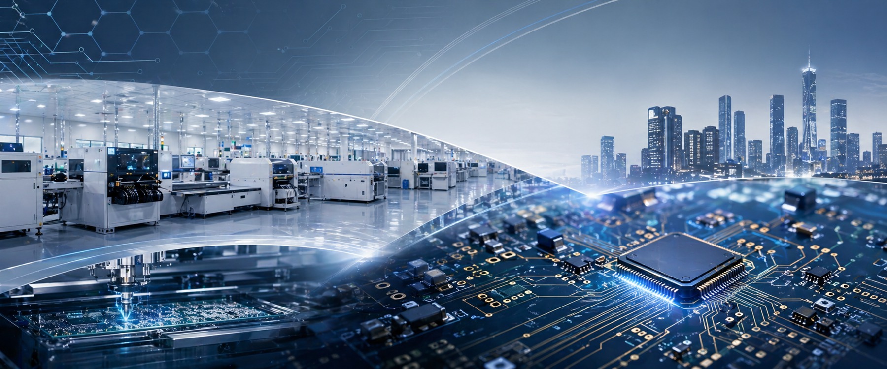
Reverse Engineering · 100% Accuracy · BOM Decryption
Professional
Professional
PCB Cloning
Services
Expert reverse engineering services to convert physical PCB samples into complete CAD files, Schematics, and BOM lists with guaranteed 100% precision.
100%AccuracySchematic Recovery
24/7SupportIC Decryption
✦Reverse EngineeringExpert Analysis
✦BOM RecoveryFull Component Lists
✦Schematic DesignFrom Physical to Digital
✦IC DecryptionFull Code Extraction
Cloning Solutions
Reverse Engineering Scope
Comprehensive cloning services for all types of electronic hardware
01
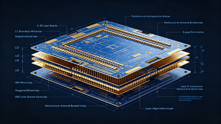
Multilayer PCB Cloning
Advanced techniques to clone complex 4-32 layer boards, including HDI structures and blind/buried vias.
- Layer-by-layer scanning
- Precise via mapping
- High-density interconnects
02
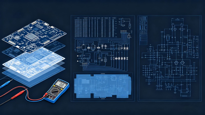
Schematic Recovery
Re-creating accurate circuit diagrams from the physical board or Gerber files for future modifications.
Learn More →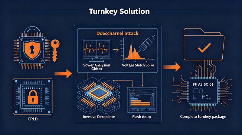
03
IC & MCU Decryption
Extracting firmware from protected microcontrollers and CPLDs to provide a complete turnkey solution.
Details →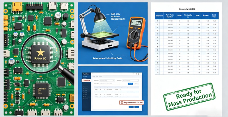
04
BOM List Generation
Full component identification including hard-to-find parts, providing a complete bill of materials for mass production.
- Component sourcing
- Obsolete part replacement
- Accurate part numbering
Capabilities
Technical Excellence
Our cloning accuracy and technical limitations
Up to 32
Layer Capability
From simple to complex HDI
0.01mm
Scanning Precision
Micron-level detail
100%
Netlist Accuracy
Software verified netlists
Gerber/CAD
Output Formats
Altium, Allegro, PADS
MCU/CPLD
Decryption Support
Most major chip brands
DFM Check
Final Validation
Production ready files
Service Contrast
Cloning vs Redesign
Choosing the right approach for your legacy hardware
| Factor | Pure Cloning | Cloning + Mod | Optimization |
|---|---|---|---|
| Functionality | Identical to Original | Modified/Improved | Enhanced Performance |
| Time to Market | Fastest | Moderate | Balanced |
| BOM Cost | Original Cost | Lowered | Optimized Cost |
| Legacy Support | Perfect for Obsolescence | Upgraded Tech | Future Proofed |
Work Flow
How We Clone
A step-by-step breakdown of our reverse engineering process
01
Sample Analysis
Detailed inspection of the physical sample and creation of the preliminary BOM list (Bill of Materials).
02
Layer Scanning
Precise removal of components and high-resolution scanning of each copper layer to capture trace routing.
03
Vectorization
Converting scanned images into CAD data (Gerber files) and reconstructing the full netlist and schematics.
04
Verification & Prototype
Manufacturing a prototype from the new files to verify 100% functional equivalence with the original.
Portfolio
Cloning Projects
Explore our successful reverse engineering cases across various industries
FAQ
1. What is PCB cloning?
PCB cloning is the process of reverse engineering an existing PCB to recreate its design data, including PCB layout, schematics, Gerber files, and bill of materials (BOM), so the board can be reproduced or manufactured again.
2. When is PCB cloning needed?
PCB cloning is typically needed when original design files are unavailable, the PCB is obsolete, or the original manufacturer no longer supports the product. It is also used to verify designs or create backups of legacy boards.
3. What data can be recovered during PCB cloning?
Depending on the board complexity, PCB cloning can recover: PCB layout and Gerber files Schematic diagrams Bill of materials (BOM) Stack-up and layer information Key component footprints
4. Is PCB cloning the same as PCB redesign?
No. PCB cloning focuses on accurately copying the existing board, while PCB redesign involves modifying the circuit or layout to improve performance, reduce cost, or replace obsolete components. Cloning preserves original functionality; redesign changes it.
5. How accurate is PCB cloning?
Accuracy depends on board condition, layer count, and component density. With professional reverse engineering, high accuracy can be achieved, and the cloned PCB can be made fully manufacturable and functionally equivalent to the original board.
Knowledge Center
Cloning Insights
Guides and news about PCB reverse engineering and hardware security

Revive Your Legacy Electronics
Don't let obsolete hardware stop your production. We turn physical boards into digital blueprints. Send us a photo or sample for a free evaluation.