Table of Contents
The Intersection of Electronics and Mechanics
Traditional rigid PCBs are static; once mounted, they don’t move. But what happens when your electronics must fold into a tiny medical wearable, twist inside a robotic arm, or endure the constant vibrations of an aerospace engine? You turn to Rigid-Flex technology.
Rigid-Flex boards combine the stability of standard FR4 with the dynamic versatility of Polyimide (PI) flexible circuits. However, designing them is notoriously difficult because you are no longer just an electrical engineer—you are now a mechanical engineer. In this article, we will break down the essential rigid flex PCB design rules required to prevent cracked traces, delamination, and catastrophic field failures, ensuring your design survives its intended lifecycle.
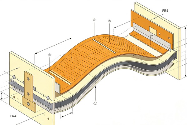
Understanding the Rigid-Flex Architecture and Materials
A typical rigid-flex board is not simply two rigid boards connected by a ribbon cable. The flexible polyimide layers are integrated directly into the stackup of the rigid sections.
The Core Materials
- Polyimide (PI): The backbone of the flex section. PI possesses incredible tensile strength, thermal stability (withstands reflow soldering), and chemical resistance.
- Rolled Annealed (RA) Copper: For dynamic flexing, RA copper is preferred over Electrodeposited (ED) copper. Its horizontal grain structure allows it to bend millions of times without fracturing.
- Coverlay vs. Solder Mask: You do not use standard liquid photoimageable (LPI) solder mask on the flexible section; it will crack instantly. Instead, a flexible Polyimide Coverlay is laminated over the traces for protection.
The Critical Transition Zone
The most vulnerable area of any rigid-flex design is the Transition Zone—the exact line where the rigid FR4 material ends and the flexible polyimide continues. This junction acts as a severe stress concentrator. If a board is going to fail mechanically, 90% of the time, it fails right at the transition zone.
Dynamic vs. Static Flexing
Before routing, you must define the application type:
* Static (Bend-to-Install): The board is bent once during assembly to fit into the enclosure and rarely moves again. The rules here are slightly more forgiving.
* Dynamic: The board will constantly flex during its operational life (e.g., a laptop hinge or a robotic actuator). The design rules here must be strictly enforced to survive millions of bend cycles.
How to Design for Rigid-Flex (Critical Design Rules)
Follow these engineering rules.
- Calculate the Minimum Bend Radius
Never fold a flex circuit like a piece of paper. The minimum bend radius dictates how tightly you can bend the board without breaking the copper.
Single/Double-Sided Dynamic Flex: Bend radius should be 10 to 20 times the total thickness of the flexible section.
Static Flex: Bend radius can be pushed to 10 times the thickness.
(Example: If your flex section is 0.2mm thick, your absolute minimum dynamic bend radius is 2.0 mm- 4.0 mm). - Protect the Transition Zone
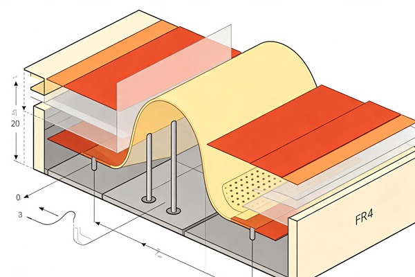
Never place vias, plated through-holes, or surface mount components within 0.1 inches (2.54mm) of the transition zone. The mechanical stress at this boundary will rip vias apart and snap component solder joints. Manufacturers usually add a bead of epoxy or silicone (strain relief) at this junction.
- Use Teardrops and Radiused Traces
A 90-degree trace corner is a stress riser. When the board flexes, the copper will crack exactly at the sharp inner corner. Always use smooth, sweeping arcs to route traces in the flex area. Furthermore, add teardrops to all via and pad connections to reinforce the copper joint where it meets the annular ring.
- Stagger Your Traces (Double-Sided Flex)
If you have copper traces on both the top and bottom of the flex material, **do not route them directly over one another**. This creates localized rigidity (known as the “I-beam effect”) and increases the chance of fracture. Instead, stagger the traces so they alternate spaces, distributing the stress evenly.
- Utilize Cross-Hatched Copper Pours
Solid copper ground planes make the flex area incredibly stiff and prone to cracking. Replace solid copper pours with a hatched or meshed grid pattern in the flexible regions. A typical ratio is a 0.2mm trace with a 0.4mm window. This maintains electrical shielding while vastly improving flexibility.
To achieve maximum mechanical reliability and comply with IPC-2223 standards, integrate these rigid flex PCB design rules into your CAD environment.
Advanced Considerations: High-Speed and HDI
Combining rigid-flex with cutting-edge electrical requirements adds another layer of complexity.
If you are routing multi-gigabit signals across a flex boundary, you must ensure the impedance remains stable. The dielectric constant of Polyimide (PI) is different from FR4 (typically around 3.2 vs 4.4), and replacing a solid ground plane with a hatched ground plane alters the trace capacitance. You must use a 3D field solver to recalculate the trace width specifically for the flexible section to maintain that 85-ohm or 100-ohm impedance. For deeper insights into signal integrity, read our guide on Essential High Speed PCB Routing Techniques.
Furthermore, if your rigid sections require extreme miniaturization, you can integrate Any Layer HDI PCB Manufacturing within the rigid zones, keeping the flexible layers limited to just 1 or 2 routing layers to maximize bendability.
Frequently Asked Questions (FAQ)
A stiffener is an extra piece of rigid material (usually FR4, Polyimide, or Stainless Steel) glued to a specific area of the flexible circuit. It is used to provide mechanical support under heavy components (like connectors) or to thicken the edge of the flex circuit so it can be inserted into a ZIF (Zero Insertion Force) connector.
Yes, but with caveats. Components on the flex area should be small and oriented so their longest dimension is parallel to the bend axis to minimize stress on the solder joints. Additionally, you must use stiffeners underneath high-pin-count components or heavy connectors to prevent the flex material from tearing.
It is highly discouraged. ED copper has a vertical grain structure that is prone to micro-cracking under repeated stress. Rolled Annealed (RA) copper, with its horizontal grain structure, is vastly superior for dynamic flexing.
Conclusion
Mastering rigid flex PCB design rules bridges the gap between electrical functionality and mechanical survival. By meticulously managing the bend radius, reinforcing the transition zones, staggering traces, and softening geometric corners, engineers can design highly dynamic interconnects that survive the harshest environments. While the design phase is undeniably more demanding, the resulting product footprint reduction and reliability gains are well worth the effort.