Table of Contents
Introduction to PCIe Gen 6 Signal Integrity Challenges
The transition to Peripheral Component Interconnect Express (PCIe) Generation 6 introduces unprecedented challenges in high-speed printed circuit board (PCB) design. Operating at 64 GigaTransfers per second (GT/s) and utilizing Pulse Amplitude Modulation 4-level (PAM4) signaling, PCIe Gen 6 demands stringent signal integrity (SI) management. PAM4 encodes two bits per symbol using four voltage levels, which significantly reduces the signal-to-noise ratio (SNR) and eye height compared to the Non-Return-to-Zero (NRZ) signaling used in previous generations.
In this high-frequency, low-margin environment, even picoseconds of phase mismatch between the positive (P) and negative (N) traces of a differential pair can completely collapse the signal eye diagram. This phase mismatch, commonly referred to as skew, translates to differential-to-common mode conversion, increased electromagnetic interference (EMI), and devastating insertion loss resonances. To guarantee robust link training and low bit error rates (BER), PCB engineers must implement rigorous skew compensation strategies, with a particular focus on mitigating the Fiber Weave Effect (FWE) and executing exacting length matching protocols.
Understanding Skew in High-Speed Differential Pairs
Skew in differential pairs manifests in two primary forms: in-pair skew and pair-to-pair skew. For serial links like PCIe Gen 6, which embed clock recovery within the data stream, in-pair skew is the most critical parameter to control.
In-Pair Skew (Intra-Pair Skew)
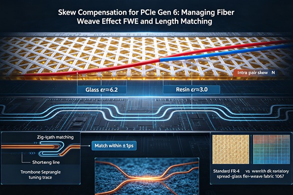
In-pair skew is the difference in propagation delay between the non-inverting and inverting traces of a single differential pair. Ideally, signals launched simultaneously should arrive at the receiver precisely at the same time and 180 degrees out of phase. When skew occurs, the signals no longer cancel out perfectly. This misalignment results in a portion of the differential signal being converted into a common-mode signal. Common-mode signals are highly undesirable as they do not benefit from the noise immunity of differential signaling, increase EMI emissions, and create resonance dips in the differential insertion loss (SDD21) profile. For PCIe Gen 6, the total allowable in-pair skew budget across the entire channel is typically on the order of a few picoseconds.
Factors Contributing to Skew
Several factors contribute to in-pair skew in PCB routing:
– Asymmetrical Routing: Mismatched trace lengths due to uncompensated bends, vias, or component breakouts.
– Glass Weave Variations: The microscopic inconsistencies in the PCB substrate materials.
– Copper Surface Roughness: Variations in the physical profile of the copper trace, though typically a secondary factor for phase.
– Connector and Package Discontinuities: Pinout geometries that inherently introduce length disparities.
The Fiber Weave Effect (FWE) Explained
In high-speed PCB fabrication, the dielectric material is typically composed of a fiberglass reinforcement matrix impregnated with an epoxy resin (such as FR4, Megtron, or Rogers materials). The fiberglass provides structural rigidity, while the resin acts as the binder. However, these two materials possess significantly different dielectric constants (Dk). The glass fibers generally have a higher Dk (around 6.0) compared to the surrounding resin (around 3.0).
The Microscopic Dielectric Imbalance
When routing differential pairs over this heterogeneous substrate, the physical alignment of the traces relative to the glass weave becomes a critical variable. If the positive trace of a differential pair is routed directly over a dense glass bundle while the negative trace is routed over a resin-rich gap (the “window”), the two signals will experience different effective dielectric constants.
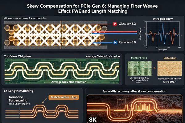
Because the velocity of propagation of an electromagnetic signal is inversely proportional to the square root of the dielectric constant, the signal traveling over the higher-Dk glass bundle will propagate slower than the signal traveling over the lower-Dk resin gap. This velocity disparity introduces a propagation delay difference, generating in-pair skew entirely independent of the physical trace length. This phenomenon is known as the Fiber Weave Effect (FWE).
At 32 GHz Nyquist frequencies for PCIe Gen 6, even minor FWE-induced skew can consume the entire error budget. Standard glass weaves like 106 or 1080 have pronounced gaps between bundles, making them highly susceptible to FWE.
Mitigation Strategies for FWE
To manage FWE in PCIe Gen 6 designs, PCB engineers must employ one or a combination of the following techniques: Learn more about BGA Underfill: Enhancing PCBA Reliability Against Mechanical Shock and Thermal Stress.
- Mechanically Spread Glass: Utilizing advanced laminates that feature mechanically spread or flattened glass yarns (e.g., 1078, 1086, 2116, 3313 weaves). These weaves minimize the resin windows, presenting a more homogeneous Dk profile to the traces.
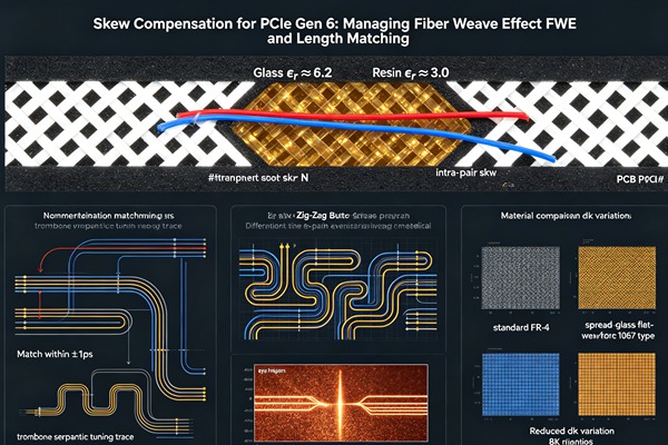
- Diagonal Routing: Routing high-speed traces at an angle (typically 10 to 15 degrees) relative to the primary X-Y axis of the PCB weave. This ensures both traces cross alternating glass bundles and resin gaps equally, averaging out the Dk variations over the length of the run.
- Zig-Zag Routing: If diagonal routing is unfeasible due to board shape or density constraints, routing in a subtle zig-zag pattern can achieve a similar averaging effect.
- Rotated Artwork: The PCB fabricator can rotate the entire panel artwork by a specific angle relative to the laminate sheet during manufacturing, effectively simulating diagonal routing for orthogonal traces.
Precision Length Matching and Phase Compensation
While mitigating FWE stabilizes the propagation velocity, physical trace lengths must still be painstakingly matched to eliminate geometric skew. For PCIe Gen 6, simple length matching is insufficient; true phase compensation must be achieved.
Phase Compensation at the Source
A fundamental rule of high-speed routing is that length mismatches must be compensated exactly where they occur. If a mismatch is generated at a BGA breakout or a connector pin, the compensation meander (or “trombone” or “accordion” structure) must be placed immediately adjacent to that discontinuity.
If a length mismatch is allowed to propagate down the channel before being corrected, the differential-to-common mode conversion will have already taken place. The common-mode signal will travel at a slightly different velocity than the differential signal due to the modal dispersion characteristics of microstrips and striplines. Compensating at the far end may fix the DC length, but it will fail to realign the AC phase across the entire frequency band. Learn more about Extreme Thermal Cycling: Reliability Testing and Material Selection for Aerospace PCBs.
Corner and Bend Management
When a differential pair navigates a corner, the outer trace inherently traverses a longer distance than the inner trace. For PCIe Gen 6, these bends must be tightly managed. High-speed designers typically utilize uncoupled bumps or specialized phase-matching geometries immediately following a bend to equalize the electrical length. Alternatively, utilizing tight coupling and smooth arcs rather than sharp 45-degree angles can minimize the differential impedance discontinuity and localized skew generation.
How to Implement Skew Compensation for PCIe Gen 6 (Step-by-Step Guide)
Follow these engineering rules.
- Select the Appropriate Dielectric Material and Glass Weave
Begin by consulting with your PCB fabricator and laminate supplier. Specify ultra-low loss materials with a flat or mechanically spread glass weave architecture (such as 2116 or 3313). Ensure the material’s Dk and Df characteristics are stable across the frequency spectrum up to at least 40 GHz.
- Define the Routing Strategy for FWE Mitigation
Determine how FWE will be addressed based on your board’s form factor and manufacturing constraints. If the layout permits, establish a global design rule to route all PCIe Gen 6 differential pairs at a 10 to 15-degree angle relative to the orthogonal axes. If not, mandate zig-zag routing or negotiate panel rotation with the manufacturer.
- Establish Stringent In-Pair Length Matching Rules
Configure your EDA tool’s constraint manager to enforce aggressive in-pair length matching rules. For 64 GT/s operation, the in-pair dynamic phase tolerance should be constrained to less than 1 picosecond (which translates to roughly 5-6 mils depending on the Dk). Set up dynamic phase checking rather than static length checking to ensure continuous alignment.
- Perform Localized Phase Compensation
Route the differential pairs meticulously, ensuring that any geometric mismatch introduced by component pads, via transitions, or bends is corrected immediately. Use tight, localized meanders. Avoid large, sweeping compensation structures that can introduce unwanted capacitive or inductive coupling.
- Validate through 3D Electromagnetic Simulation
Before finalizing the layout, extract the critical PCIe Gen 6 channels using a 3D full-wave electromagnetic (EM) solver. Analyze the mixed-mode S-parameters, specifically focusing on the differential insertion loss (SDD21) and the differential-to-common mode conversion (SCD21). Look for sharp resonance dips in the SDD21 profile, which often indicate uncompensated phase skew. Re-iterate the layout based on simulation feedback until the channel meets the PCIe Gen 6 compliance mask.
Implementing a robust skew compensation strategy requires a systematic approach from schematic capture through physical layout and simulation. Follow these steps to ensure compliance with PCIe Gen 6 specifications.
Advanced Considerations for 64 GT/s Channels
As data rates continue to scale, the definition of a “trace length” becomes complex. PCB design tools must account for the Z-axis transitions as well. The length of vias, especially the distance from the top layer to internal signal layers, introduces localized delays that must be symmetrically matched.
Via Stub Management
For PCIe Gen 6, via stubs act as resonant antennas and must be strictly controlled. Backdrilling (controlled depth drilling) or using blind/buried vias is mandatory to eliminate resonant stubs that can create deep nulls in the channel’s insertion loss profile. When compensating for skew near vias, ensure the compensation structure takes into account the electrical length of the via barrel itself. Learn more about Embedded Components: Miniaturizing IoT Devices with Embedded PCB Components.
Surface Roughness Impact
While FWE dictates phase variation, copper surface roughness profoundly impacts insertion loss at 32 GHz Nyquist frequencies. The “skin effect” forces high-frequency currents to travel along the outer surface of the copper trace. Rougher copper treatments (like standard RTF) increase the effective path length, causing excessive attenuation and phase dispersion. Specify low-profile (LP), very low-profile (VLP), or hyper-low-profile (HVLP) copper foils to preserve signal integrity and minimize unpredictable phase shifts caused by roughness variations.
Conclusion
Designing PCBs for PCIe Gen 6 requires a paradigm shift in how engineers approach signal integrity. The sheer speed of 64 GT/s PAM4 signaling drastically reduces the tolerance for any channel imperfections. Managing in-pair skew is no longer just about matching trace lengths on a 2D plane; it requires a holistic approach that comprehends the 3D geometry of the interconnect, the microscopic structure of the dielectric materials, and the dynamic behavior of electromagnetic waves. By rigorously managing the Fiber Weave Effect, implementing localized phase compensation, and relying on advanced EM simulation, engineers can successfully deploy robust and reliable PCIe Gen 6 architectures. Learn more about Return Path Optimization: Designing Solid Reference Planes for High-Frequency Signal Integrity.
Frequently Asked Questions (FAQ)
While the exact budget depends on the entire channel’s composition (silicon packages, connectors, cables), the typical rule of thumb for the PCB portion of a PCIe Gen 6 link is to maintain in-pair skew below 1 to 2 picoseconds (approximately 5 to 10 mils of trace length, depending on the material). Even this small amount can degrade the PAM4 eye diagram significantly.
If skew is introduced early in the channel (e.g., at the transmitter package breakout), it creates a common-mode signal component. Because differential and common-mode signals propagate at slightly different velocities in standard PCB cross-sections, the phase relationship drifts as the signal travels. Compensating at the far end might match the physical length but will fail to re-align the differential phase correctly across all frequencies, leading to signal degradation.
Diagonal routing (off-axis routing) is generally considered superior and more consistent for mitigating FWE. Zig-zag routing can sometimes introduce minor impedance discontinuities at the inflection points, especially if the zig-zag segments are short relative to the signal wavelength. However, if board space or shape prevents diagonal routing or panel rotation, zig-zag routing is a viable alternative when properly simulated.
PCIe architecture inherently manages pair-to-pair skew (lane-to-lane skew) at the protocol and silicon level through a process called lane deskewing during link training. Therefore, PCB designers have much looser tolerances for pair-to-pair length matching (often up to several inches) compared to the ultra-tight constraints required for in-pair skew.
PAM4 uses four voltage levels to transmit two bits per symbol, which reduces the vertical eye height (Signal-to-Noise Ratio) by approximately a factor of three compared to NRZ signaling used in PCIe Gen 5 and earlier. With significantly less margin for noise and jitter, any distortion introduced by phase skew has a disproportionately severe impact on the bit error rate (BER) in a PAM4 system.