Table of Contents
Introduction to BGA Underfill and PCBA Reliability
As printed circuit board assemblies (PCBAs) continue to miniaturize and incorporate higher-density interconnects (HDI), the utilization of Ball Grid Array (BGA), Chip Scale Package (CSP), and Wafer-Level Chip Scale Package (WLCSP) components has become ubiquitous across the electronics manufacturing sector. While these packaging technologies offer superior electrical performance, shorter signal paths, and densely packed I/O configurations, they present significant and complex mechanical challenges. The fundamental structural vulnerability lies in the integrity of the SMT solder joints that interface the rigid silicon package with the comparatively flexible FR-4 or polyimide PCB substrate. To aggressively mitigate these vulnerabilities, hardware engineers and manufacturing specialists employ BGA underfill—a specialized, highly engineered epoxy encapsulant designed to completely fill the interstitial space between the component die and the board substrate, fully encapsulating the solder spheres.
The primary function of BGA underfill is to transition the structural and mechanical load away from the fragile solder joints and distribute it evenly across the entire surface area of the component footprint. In high-reliability and mission-critical applications, such as automotive control modules, aerospace avionics, telecommunications infrastructure, and ruggedized industrial electronics, unprotected solder joints are highly susceptible to fatigue, micro-fracture, and ultimate failure induced by extreme thermal cycling, mechanical shock drops, and continuous harmonic vibration. By essentially coupling the BGA rigidly to the substrate substrate, underfill drastically enhances the survivability of the PCBA under extreme operational stresses, ensuring the longevity and reliability of the final product.
The Physics of Solder Joint Failure in High-Density Packages
To fully appreciate the necessity and engineering behind BGA underfill, one must deeply understand the failure mechanics inherent to surface-mount technology (SMT) solder joints, particularly those involving distinct material layers with divergent thermomechanical properties.
Coefficient of Thermal Expansion (CTE) Mismatch
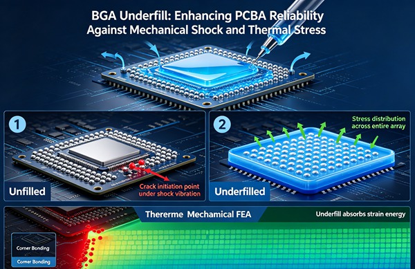
The most pervasive and unavoidable threat to BGA reliability is thermal cycling. A typical bare silicon die exhibits a Coefficient of Thermal Expansion (CTE) of approximately 2.6 ppm/°C. Conversely, a standard FR-4 PCB substrate has a CTE ranging from 14 to 18 ppm/°C in the X-Y plane. When the PCBA undergoes substantial temperature fluctuations—whether from ambient environmental changes or intense internal power cycling from the IC itself—the substrate expands and contracts at a significantly higher rate than the rigid silicon package.
This profound CTE mismatch generates immense shear stress across the solder joints connecting the two disparate materials. Over repeated thermal cycles, this strain energy accumulates, initiating micro-cracks at the stress concentration points. These stress risers are typically located near the pad-to-solder interface or within the brittle intermetallic compound (IMC) layer that forms between the copper pad and the solder alloy. As thermal cycling continues relentlessly, these microscopic cracks propagate entirely through the bulk solder, eventually resulting in a complete electrical open circuit and system failure. BGA underfill directly mitigates this by possessing a CTE engineered to bridge the gap between the silicon and the FR-4, effectively locking the assembly together and suppressing the localized shear strain on individual solder bumps.
Mechanical Shock and Vibrational Fatigue
Beyond thermal stress, modern portable electronics and automotive assemblies are repeatedly subjected to severe mechanical shock (e.g., drop impacts) and relentless vibrations. During a dynamic drop event, the PCB experiences rapid flexure and warping. This dynamic bending creates severe tensile and compressive stresses that can easily fracture brittle solder joints in milliseconds. This is especially true for modern assemblies formulated with lead-free SAC (Tin-Silver-Copper) alloys, which are inherently more rigid, stiff, and brittle than traditional, compliant SnPb (Tin-Lead) solder. Underfill acts as a powerful mechanical shock absorber and stiffener, providing dampening and rigidity that prevents the PCB flexure from translating directly into solder joint shear.
Types of BGA Underfill Materials
The selection of an appropriate underfill material is not arbitrary; it depends heavily on the specific manufacturing process flow, the complex architecture of the component, and the intended operational environment. The three primary classifications of underfill utilized in SMT are Capillary, No-Flow, and Molded.
Capillary Underfill (CUF)
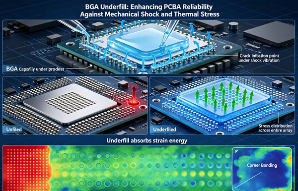
Capillary underfill represents the most widely adopted and robust methodology for post-reflow encapsulation in high-reliability manufacturing. The material—typically a heavily silica-filled, low-viscosity epoxy resin—is precisely dispensed along one or two edges of the BGA after the component has been successfully soldered to the board and passed initial inspection. Through natural capillary action, the liquid resin is aggressively drawn underneath the component, flowing seamlessly between the densely packed solder spheres until it emerges on the opposite side. This forms a continuous encapsulating layer and a crucial structural fillet around the entire package perimeter. This process relies heavily on surface tension dynamics and precise substrate heating to maintain an optimal flow viscosity.
No-Flow Underfill (NUF)
No-Flow Underfill (NUF) is integrated directly into the primary SMT assembly process, eliminating the need for a costly secondary post-reflow dispensing step. NUF is typically dispensed as a highly viscous, precisely measured droplet directly onto the BGA pad footprint on the bare PCB prior to the pick-and-place operation. The BGA component is then driven down into the underfill. During the standard reflow oven cycle, the NUF acts simultaneously as an active fluxing agent—reducing oxides on the solder spheres and PCB pads to facilitate proper metallurgical bonding—and as a robust encapsulant that thermosets and cures as the solder solidifies. While NUF significantly streamlines manufacturing, it often lacks the extremely high filler content of CUF, making it slightly less effective at maximizing CTE reduction. Learn more about Crosstalk Mitigation: Advanced Routing Techniques to Minimize NEXT and FEXT in High-Speed PCBs.
Molded Underfill (MUF)
Molded underfill is utilized primarily in advanced, ultra-dense semiconductor packaging, such as System-in-Package (SiP), heterogeneous integration modules, and advanced memory stacks. In MUF processes, a solid or highly viscous molding compound is forced into the microscopic cavities under extreme heat and pressure, encapsulating both the internal die and the BGA interconnections simultaneously. This provides maximum structural rigidity and environmental protection but is generally restricted to the component-level manufacturing phase rather than the board-level PCBA assembly phase.
Key Material Properties of Underfill
Specifying the correct underfill requires a deep dive into its unique rheological and thermomechanical properties. Selecting an incompatible underfill formulation can actually induce premature stress failure rather than prevent it.
Glass Transition Temperature (Tg)
The Glass Transition Temperature (Tg) is the critical thermal threshold where the underfill polymer matrix transitions from a rigid, glassy state to a softer, more compliant, rubbery state. Below the Tg, the underfill has a low CTE and an exceptionally high modulus, effectively restraining the BGA. Above the Tg, the material’s CTE increases dramatically, and its structural modulus drops. For maximum reliability, the underfill’s Tg should ideally be higher than the maximum continuous operating temperature of the PCBA, ensuring the material remains in its rigid, highly protective state throughout the product’s entire lifecycle. Learn more about M-SAP Technology: Achieving Sub-25 Micron Line/Space for Next-Generation Electronics.
Coefficient of Thermal Expansion (CTE)
As previously discussed, effectively bridging the CTE gap is paramount. An ideal underfill formulation will have a CTE closely matching the solder joints themselves (typically around 20-25 ppm/°C) to prevent the cured underfill from exerting independent, destructive stress on the fragile bumps. Chemical manufacturers achieve these precise target CTE values by blending the base liquid epoxy resin with microscopic, spherical silica fillers.
Young’s Modulus
Young’s Modulus dictates the stiffness and rigidity of the completely cured underfill. A high-modulus (stiff) underfill provides excellent protection against thermal fatigue by aggressively coupling the component directly to the board. However, if the modulus is excessively high, it can transfer too much mechanical stress to the delicate low-k dielectric layers within the silicon die itself, leading to catastrophic die cracking or layer delamination. Engineering the correct, balanced modulus is a complex optimization problem for material scientists.
Viscosity and Filler Content
Viscosity determines exactly how effectively a capillary underfill will flow under a tight-pitch, low-standoff component. High filler loading (often reaching up to 60-70% by weight) is absolutely necessary to lower the CTE and increase the modulus. However, adding rigid filler significantly increases fluid viscosity and hinders capillary flow speed. Advanced modern underfills utilize sub-micron silica spheres and specialized chemical rheology modifiers to achieve high filler densities while maintaining flow characteristics suitable for ultra-fine bump pitches as small as 100 microns.
How to Apply Capillary BGA Underfill (Step-by-Step Guide)
Follow these engineering rules. Learn more about Sequential Lamination: Mastering the Manufacturing Process for Any-Layer HDI Boards.
- Board Preparation and Preheat
The PCBA must be thoroughly cleaned or explicitly utilize a strictly compatible no-clean flux system, as residual unreacted flux can severely impede capillary flow and drastically reduce chemical adhesion. The entire assembly is then transferred to a heated platen or inline heating zone. Preheating the substrate to a highly specific temperature (typically between 70°C and 100°C) is essential to artificially reduce the viscosity of the underfill resin, allowing it to flow rapidly and evenly beneath the package without triggering a premature thermosetting cure.
- Precise Dispensing
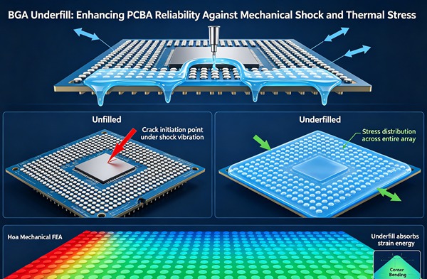
Using state-of-the-art automated fluid dispensing equipment equipped with specialized auger pumps or high-speed jetting valves, a precise, micro-calculated volume of underfill is deposited along one edge (L-pattern or I-pattern) of the BGA. The dispense needle must be positioned meticulously in the Z-axis to ensure the material contacts the component edge, initiating the crucial capillary draw, without physically colliding with the die or contaminating adjacent micro-components.
- Capillary Flow Wait Time
Once dispensed, the assembly is continuously held at the preheat temperature to allow the natural capillary action to smoothly draw the fluid completely under the package matrix. The time required depends heavily on the component dimensions, bump pitch density, Z-axis gap height, and specific material viscosity. Rushing this critical step will inevitably result in trapped air pockets (voids) under the die, which can forcefully expand during subsequent thermal cycles and cause solder joint extrusion or component delamination.
- Fillet Inspection
After the flow is deemed complete, the underfill must emerge on the opposite sides of the component, forming a continuous, perfectly concave fillet. The fillet provides critical structural support against sheer mechanical shock. Automated Optical Inspection (AOI) or high-magnification manual visual inspection is utilized to verify a complete, uniform fillet without excessive material bleed-out onto surrounding pads.
- Thermal Curing
The fully underfilled PCBA is then carefully transferred to a batch convection oven or an inline curing oven. The assembly is subjected to a rigidly controlled thermal profile (e.g., 150°C for 30 to 45 minutes) to securely cross-link the complex polymer chains and harden the epoxy into its final state. Careful attention must be paid to the temperature ramp rate to prevent rapid outgassing of any trapped volatiles, which could form internal microscopic voids within the fully cured matrix.
Proper application methodology is just as critical as the material selection itself. Inadequate processing parameters can easily lead to severe voiding, incomplete component coverage, and flux incompatibility, completely negating the intended benefits of the underfill.
Defect Analysis and Reliability Testing
Post-application, rigorous quality assurance is required to validate the underfill process. The most common defect is voiding. Voids act as severe stress concentrators. If a void happens to encompass a solder bump, the unsupported joint is highly vulnerable to fatigue, and moisture ingress within the void can lead to corrosion.
Because the underfill is hidden beneath the IC, visual inspection is impossible. Engineers rely on Scanning Acoustic Microscopy (C-SAM) to non-destructively image the underfill layer. C-SAM utilizes high-frequency ultrasonic waves to detect changes in material density, clearly revealing any trapped air pockets or areas of delamination. Learn more about Skew Compensation: Managing Fiber Weave Effect (FWE) and Length Matching for PCIe Gen 6.
For final product validation, underfilled assemblies undergo brutal reliability testing in accordance with JEDEC standards. This includes Thermal Shock Testing (e.g., rapid cycling from -40°C to +125°C) and highly accelerated Drop Testing to simulate real-world impacts, ensuring the underfill meets the required lifespan criteria.
Advanced Considerations: Reworkability and Flux Compatibility
Historically, successfully applying underfill meant the BGA was permanently and irreversibly adhered to the board, making post-assembly rework physically impossible. If a component failed test, the entire highly expensive PCBA had to be scrapped. Today, chemical manufacturers have successfully developed advanced thermally reworkable underfills. These materials are highly engineered to intentionally degrade and lose their adhesive strength when subjected to temperatures significantly above normal SMT reflow profiles (e.g., 220°C – 260°C). During a rework cycle, localized, highly controlled heat is applied, allowing the defective component to be gently lifted and the residual degraded underfill to be mechanically scraped or chemically dissolved from the PCB copper pads.
Another absolutely critical consideration is flux compatibility. When using a standard no-clean SMT process, harmless flux residues remain around the solder joints immediately after reflow. However, if the specific underfill chemistry is incompatible with the chemical makeup of that flux residue, it can lead to poor adhesion at the microscopic interfaces, localized delamination over time, or even severe electromigration (dendrite growth) issues. Extensive empirical reliability testing and compatibility qualification are required to ensure the underfill cleanly encapsulates the flux residue without any adverse long-term chemical interactions.
Frequently Asked Questions (FAQ)
Capillary underfill is applied dynamically after the SMT reflow process is complete; it relies heavily on external heat and natural capillary action to flow smoothly beneath a completely soldered component. No-flow underfill is dispensed directly onto the bare board before component placement, acting as both an active flux to aid soldering and a structural encapsulant that cures simultaneously during the standard solder reflow process. Capillary underfills generally offer superior, long-term thermomechanical protection due to their substantially higher silica filler content.
Yes, but only if a specifically formulated “reworkable underfill” was intentionally used during the original assembly. These highly engineered epoxies are designed to physically break down and release at extremely high temperatures, allowing the component to be carefully removed and the site prepared for a new IC. Standard, highly cross-linked non-reworkable underfills effectively render the BGA completely permanent; attempting rework will almost certainly rip the delicate copper pads directly from the PCB substrate.
Filler content (typically microscopic silica spheres) is added by the manufacturer to aggressively reduce the Coefficient of Thermal Expansion (CTE) and drastically increase the Young’s Modulus of the underfill, making it fundamentally better at protecting the SMT joints against severe thermal cycling. However, high filler content inherently increases the base viscosity of the uncured resin, which can severely impede capillary flow and make it exceptionally difficult to use on tightly pitched, low-standoff components.
Voiding (trapped air bubbles within the cured epoxy) can be caused by improper dispensing patterns (trapping air before it can escape), inadequate preheating of the substrate, flux outgassing during the cure cycle, or curing the material too rapidly. Voids are extremely dangerous because they act as focal points for stress. If a void is located adjacent to a solder bump, the expanding air during a thermal cycle can exert intense physical pressure on the joint, leading to premature mechanical fracture or forced extrusion of the solder into the empty void space.
No. Underfill is typically reserved specifically for fine-pitch BGAs, delicate Wafer-Level Chip Scale Packages (WLCSPs), highly massive components, or assemblies operating in exceptionally harsh environments with significant thermal cycling or relentless vibration. Standard-pitch BGAs in benign, controlled consumer environments often do not require underfill, as the solder joints themselves possess sufficient inherent compliance to successfully handle minor, everyday thermomechanical stresses.