High-Density Interconnect (HDI) technology has fundamentally transformed the printed circuit board (PCB) landscape, enabling unprecedented miniaturization, enhanced signal integrity, and superior electrical performance in modern electronics. As device architectures—ranging from cutting-edge smartphones, 5G base stations, and wearable technology to advanced automotive computing units and aerospace instrumentation—demand higher pin counts and finer pitch components, traditional PCB fabrication methods have proven insufficient. The definitive solution to these modern engineering challenges is the implementation of any-layer HDI architecture, realized through the rigorous and highly controlled manufacturing process known as sequential lamination.
Sequential lamination is not merely a fabrication step; it is a sophisticated engineering methodology that allows designers to construct a PCB layer by layer, building up complex interconnect structures that would be physically impossible using standard multilayer pressing techniques. Unlike conventional boards, where all layers are stacked and pressed in a single monolithic cycle with mechanically drilled through-holes, sequential lamination involves multiple, iterative cycles of pressing, drilling, plating, and etching. This iterative process is the absolute key to creating microvias, blind vias, and buried vias that provide optimal routing paths and minimize signal degradation. Learn more about Return Path Optimization: Designing Solid Reference Planes for High-Frequency Signal Integrity.
In the realm of any-layer HDI (also known as Every Layer Interconnect or ELIC), sequential lamination reaches its zenith. Any-layer HDI boards abandon the traditional rigid core entirely, utilizing stacked copper-filled microvias to allow connections between any two layers within the stack-up. This architectural freedom drastically reduces the layer count required for complex routing, mitigates parasitic capacitance and inductance by minimizing via stubs, and provides superior thermal management. However, mastering the sequential lamination process demands a profound understanding of materials science, photolithography, laser physics, and chemical plating dynamics. Learn more about Conformal Coating: Protecting PCBA from Moisture, Dust, and Corrosive Environments.
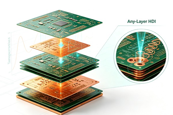
Table of Contents
The Engineering Principles of Sequential Lamination
At its core, sequential lamination relies on the precise addition of dielectric materials and copper foil to a base substrate, followed by the formation of microvias using laser ablation. The term “sequential” denotes the repetitive nature of this build-up process. A typical nomenclature for HDI stack-ups is X-N-X, where ‘N’ represents the number of core layers and ‘X’ represents the number of sequential lamination cycles on each side of the core. For instance, a 3+4+3 stack-up involves a 4-layer core with three sequential build-up layers on the top and three on the bottom. In any-layer HDI, the architecture might be a pure sequential build without a traditional core, often denoted simply by the total layer count, such as a 10-layer or 12-layer ELIC board.
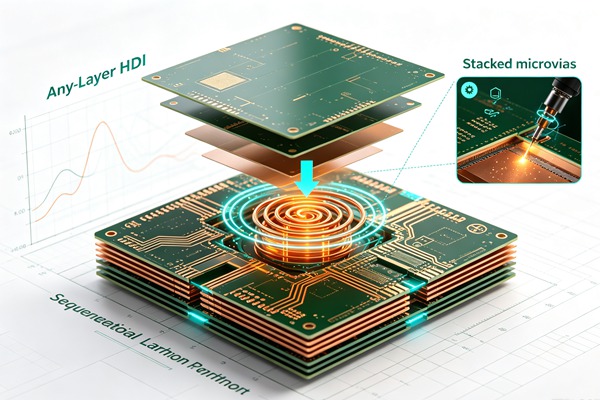
The primary driver for employing sequential lamination is the creation of microvias—holes typically 150 micrometers or less in diameter. Mechanical drilling is fundamentally incapable of reliably producing vias of this scale, necessitating the use of Ultraviolet (UV) or Carbon Dioxide (CO2) lasers. The sequential approach ensures that these lasers only need to penetrate a single dielectric layer at a time, allowing for tight aspect ratios, impeccable registration, and precise depth control. Furthermore, by filling these microvias with solid copper during the plating phase, manufacturers can stack vias directly on top of one another, a critical requirement for any-layer interconnects that route signals vertically through the exact same X-Y coordinate. Learn more about Extreme Thermal Cycling: Reliability Testing and Material Selection for Aerospace PCBs.
This multi-step approach introduces significant mechanical and thermal stresses to the board. The CTE (Coefficient of Thermal Expansion) mismatch between the copper layers (around 17 ppm/°C), the dielectric resin, and the glass reinforcement can lead to warpage, delamination, or via barrel cracking during the high temperatures of the lamination press or subsequent reflow soldering. Therefore, the selection of advanced prepreg materials and precise control over the lamination press cycles (temperature, pressure, and vacuum profiles) are paramount to ensuring the structural integrity of the final product.
How to Manufacture Any-Layer HDI Boards Using Sequential Lamination (Step-by-Step Guide)
Follow these engineering rules. Learn more about Stacked vs. Staggered Microvias: Design Rules and Reliability in High-Density Interconnect (HDI) PCBs.
- Core Preparation and Initial Imaging
While true any-layer HDI might start with a highly thin core or build upon a temporary carrier that is later removed, standard sequential lamination begins with the preparation of an inner core. A copper-clad laminate (CCL) is chemically cleaned and micro-etched to promote photoresist adhesion. Dry film photoresist is laminated onto the copper surfaces, exposed to UV light through a highly precise photomask, and developed to reveal the desired circuitry pattern. The exposed copper is then chemically etched away, leaving the inner layer traces. The resist is stripped, and the remaining copper undergoes an oxide treatment (such as brown oxide or alternative oxide formulations) to increase surface roughness, creating a micro-toothed structure that ensures maximum bond strength with the dielectric in the subsequent lamination step.
- First Lamination Cycle and Pressing
A layer of un-cured dielectric material (prepreg), often combined with a sheet of copper foil (in a foil-build configuration), is precisely aligned over the etched core using sophisticated tooling pins and optical alignment. This assembly is placed into a vacuum lamination press. Under strict vacuum conditions to eliminate air entrapment, the stack is subjected to a meticulously profiled cycle of heat and pressure. The resin in the prepreg melts (reaching its lowest viscosity), flows to encapsulate the inner layer circuitry without leaving voids, and then fully cures and polymerizes as the temperature increases. The vacuum is critical here; any trapped voids will expand exponentially during later thermal processes, leading to catastrophic delamination or serving as failure points during laser drilling.
- Laser Drilling Microvias
Once the first lamination cycle is complete, the board transitions to the laser drilling station. For advanced HDI, a combination of UV and CO2 lasers is frequently employed in a dual-laser system. The UV laser is used to precisely ablate the top copper foil (creating a defined opening window), while the CO2 laser ablates the underlying dielectric material down to the target copper pad on the layer below. The CO2 laser’s wavelength is highly reflective to copper, allowing it to ablate the resin and stop precisely on the target pad. The laser parameters—including pulse energy, frequency, and focal spot size—must be stringently calibrated based on the specific dielectric material to ensure clean via formation without damaging the target pad (a defect known as punch-through) or leaving excessive residual resin.
- Desmear and Metallization (Copper Plating)
The intense heat of the laser ablation process melts the dielectric resin, leaving a thin layer of carbonized resin ash and debris (smear) at the bottom of the microvia, which would severely compromise electrical connectivity. The boards undergo a robust chemical desmear process, typically utilizing alkaline permanganate solutions at elevated temperatures, to aggressively clean and condition the via walls and the target pad. Following desmear, the boards are subjected to an electroless copper plating bath, which deposits a thin, conductive seed layer of copper over the entire surface, including inside the non-conductive dielectric vias. This is immediately followed by an electrolytic copper plating process. For any-layer HDI, specific plating additives (brighteners, levelers, and carriers) are used to achieve bottom-up “via filling,” where the microvia is plated completely solid with copper, providing a perfectly flat surface essential for stacking the next sequential layer.
- Outer Layer Imaging and Etching
With the microvias fully filled and the surface copper plated to the desired thickness, the board undergoes another cycle of photolithography. Photoresist is applied, exposed, and developed to define the circuitry for the newly added layer, including the critical capture pads that overlay the underlying stacked vias. The unwanted copper is etched away, and the resist is stripped, finalizing the conductive pattern for this specific sequential layer.
- Subsequent Lamination Cycles (The “Sequential” Process)
Steps 2 through 5 represent a single sequential build-up cycle. For an HDI board requiring multiple sequential layers, or an any-layer ELIC board, this entire sequence is repeated meticulously for each additional layer. A new sheet of prepreg and copper foil is laminated, new microvias are laser-drilled (often stacked directly onto the solid copper-filled vias of the previous layer), desmeared, plated solid, imaged, and etched. This iterative loop requires exceptional registration capabilities, as the alignment tolerances become increasingly stringent with each added layer due to cumulative material movement and scaling factors.
- Final Processing and Quality Inspection
After all sequential layers have been built and the final outer layer circuitry is defined, the board proceeds to standard final fabrication steps. This includes the application of liquid photoimageable solder mask (LPI), which must accurately align with the high-density pads and finely pitched BGA footprints. A surface finish is then applied (such as ENIG, ENEPIG, or Immersion Tin) to protect exposed copper and ensure solderability. Given the immense complexity and value of sequential lamination boards, rigorous testing is mandatory. Automated Optical Inspection (AOI) checks for trace defects at every layer, while Time Domain Reflectometry (TDR) may be used for impedance verification. Crucially, high-voltage bare board electrical testing ensures no micro-shorts or opens exist within the incredibly dense via structures.
Material Selection and Thermal Considerations
The success of sequential lamination is heavily dependent on the materials chosen. Standard FR-4 is often inadequate for advanced HDI due to its relatively high CTE, which can induce severe stress fractures in stacked microvias during thermal cycling or lead to pad lifting. Engineers must specify high-Tg (glass transition temperature, typically >170°C) and low-CTE resin systems to ensure reliability.
Furthermore, the glass weave style of the prepreg’s glass-weave style preprprepreg’s glass-weave style eg plays a significant role. Standard coarse glass weaves can cause laser deflection (the “glass knuckles” effect) and lead to uneven laser drilling, skewed vias, or incomplete ablation. To combat this, laser-drillable prepregs utilizing spread-glass technology or even unreinforced resin-coated copper (RCC) films are often employed. RCC is particularly valuable in any-layer HDI as it provides a uniform dielectric thickness and eliminates the glass weave entirely, ensuring consistent via geometries and dramatically improving signal integrity by reducing the local dielectric constant variations and eliminating the fiber weave effect (skew) on high-speed differential pairs.
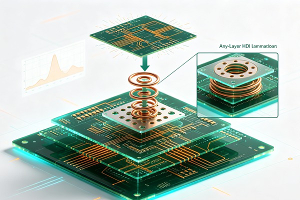
Thermal management is another critical vector. While stacked microvias offer excellent thermal conductivity compared to standard FR-4 (acting essentially as thermal vias), the extreme density of components on any-layer HDI boards generates significant localized heat. Thermal modeling during the design phase must account for the specific thermal resistance of the sequential stack-up. Selecting dielectric materials with higher thermal conductivity can mitigate localized hot spots and ensure long-term reliability in harsh operating environments, preventing thermal runaway in high-power integrated circuits.
Challenges and Yield Optimization Strategies
Sequential lamination is inherently more expensive, time-consuming, and challenging than standard multilayer pressing. The primary challenge is yield loss; because the process is iterative, a defect occurring on the final lamination cycle effectively scraps the entire board, wasting all prior processing effort, time, and premium materials.
Registration scaling is a constant and demanding battle. As the board undergoes repeated cycles of high heat and pressure during each lamination phase, the materials expand, contract, and permanently deform, altering the dimensional stability of the panel. Manufacturers must utilize advanced predictive scaling software that accounts for warp and fill material properties, alongside high-precision CCD camera alignment systems at every imaging and drilling step to dynamically compensate for this material movement.
Furthermore, the chemical control of the via-filling plating baths must be extraordinarily precise. The fluid dynamics within a 100-micrometer blind via are complex. The plating chemistry must accurately deposit copper from the bottom up without bridging over the top and trapping chemistry inside. Ensuring void-free copper deposition in the stacked vias is critical, as any trapped void can lead to violent outgassing and via barrel failure (blowholes) during high-temperature assembly reflow processes. Continuous monitoring of plating bath concentrations, organic additives, and current density profiles is required to maintain peak yield.
The manufacturing of any-layer HDI boards via sequential lamination is an intricate, highly controlled sequence of operations. Every cycle must be executed flawlessly to prevent compounded errors. This section details the fundamental steps involved in building up the interconnect structures.
Frequently Asked Questions (FAQ)
A standard blind via connects the outer layer to an inner layer and is usually formed by drilling through a single dielectric layer. A stacked microvia, achievable only through sequential lamination and highly specialized bottom-up via-filling copper plating, involves placing multiple microvias directly on top of one another across successive layers. This is essential for any-layer HDI, allowing a vertical connection straight through the board without staggering the vias, thereby saving vital routing space and improving high-frequency signal integrity.
Mechanical drill bits become highly fragile and economically unviable at diameters below 150 micrometers. Furthermore, mechanical drilling cannot reliably control depth (Z-axis) to stop precisely on a target copper pad just microns below the surface without causing damage. Laser drilling provides the necessary non-contact precision, exact ablation depth control, and micro-scale diameters required for manufacturing HDI microvias reliably at scale.
Sequential lamination significantly increases the manufacturing lead time. A standard multilayer board requires only one primary lamination press cycle and one main drilling and plating cycle. In contrast, a sequential board requires a full cycle of pressing, laser drilling, desmear, plating, and etching for *each* sequential layer added. Therefore, an HDI board with a 3+4+3 stack-up will require substantially more fabrication time and labor than a standard 10-layer board.
No, sequential lamination principles are extensively used in rigid-flex and pure flexible printed circuits as well. High-density flex circuits often require microvias and complex routing that benefit from sequential build-up techniques. These applications utilize specialized flexible dielectrics like polyimide instead of rigid FR-4 prepregs, requiring highly specialized handling and processing parameters adapted for flexible materials.
ELIC stands for Every Layer Interconnect. It is a specific, highly advanced type of HDI board architecture where every layer is built up sequentially, usually without a thick central rigid core. It relies entirely on stacked, solid copper-filled microvias, allowing for electrical connection between any two layers in the entire stack-up. ELIC represents the most complex and capable application of the sequential lamination manufacturing process, widely used in premium smartphones and ultra-compact devices.