In the realm of advanced printed circuit board (PCB) design, engineers often focus heavily on the routing of signal traces—meticulously tuning lengths, matching impedances, and routing differential pairs with extreme precision. However, a signal trace is only one half of the electrical equation. Every electrical signal requires a complete closed loop to flow, meaning the return current must find its way back to the source. The route this return current takes is known as the return path, and its management is critical. Return path optimization is arguably the most crucial aspect of ensuring high-frequency signal integrity in modern electronics.
As switching speeds increase and edge rates become faster in contemporary digital and RF systems, the behavior of return currents shifts dramatically. Failing to provide a continuous, low-impedance return path leads to a host of signal integrity (SI) and electromagnetic interference (EMI) issues, ranging from severe crosstalk and ground bounce to unacceptable levels of radiated emissions. Designing solid reference planes is the foundational strategy for mitigating these issues and ensuring reliable, high-performance PCB operation.
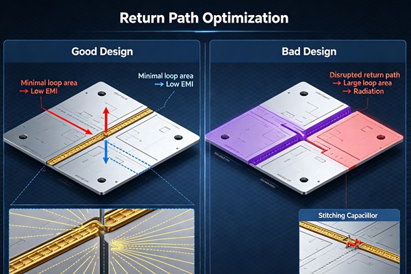
The Physics of Return Currents: Resistance vs. Inductance Learn more about AOI & 3D X-Ray: Achieving Zero-Defect PCB Assembly.
To master return path optimization, one must first understand how current behaves at different frequencies. The fundamental rule of electricity states that current always takes the path of least impedance. Impedance ($Z$) comprises both resistance ($R$) and reactance ($X$), heavily influenced by inductance ($L$) at higher frequencies ($Z = R + j\omega L$, where $\omega$ is the angular frequency). Learn more about PCBA SMT Assembly: Mastering Fine-Pitch BGA and 01005 Components.
At direct current (DC) or very low frequencies, the reactive component is negligible. Therefore, the return current takes the path of least resistance. In a solid ground plane, the DC return current spreads out widely, taking a direct, straight-line path from the load back to the source, regardless of how the signal trace is routed on the layers above.
However, as the frequency increases (typically above 100 kHz, and certainly into the MHz and GHz ranges characteristic of modern high-speed designs), the inductive reactance dominates the impedance equation. High-frequency AC return current no longer takes the path of least resistance; it takes the path of least inductance. The lowest inductance path is achieved by minimizing the loop area between the outgoing signal path and the returning current path. Consequently, high-frequency return currents concentrate directly underneath the signal trace on the adjacent reference plane. This phenomenon is known as the proximity effect. When a trace routes tightly over a solid, uninterrupted reference plane, the return current forms a tight, concentrated band right beneath it, minimizing the loop inductance and ensuring optimal signal integrity. Learn more about Conformal Coating: Protecting PCBA from Moisture, Dust, and Corrosive Environments.
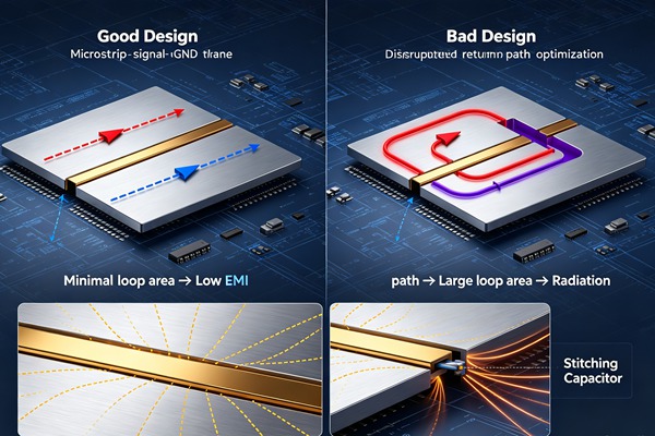
Table of Contents
The Impact of Discontinuous Return Paths
When the path of least inductance is interrupted, the return current is forced to deviate from its ideal path beneath the signal trace. This diversion increases the physical loop area, which directly increases the loop inductance. An increased loop area acts as a highly efficient loop antenna, radiating electromagnetic energy and causing severe EMI issues.
Furthermore, discontinuities in the return path degrade signal integrity in several specific ways:
– Impedance Discontinuities: The characteristic impedance of a trace is calculated based on its geometry relative to the nearest reference plane. If the plane is interrupted (e.g., crossing a split), the capacitance to the reference plane drops, causing a sudden spike in characteristic impedance. This mismatch results in signal reflections, ringing, and degraded eye diagrams.
– Crosstalk Escalation: When return currents from multiple signals are forced to navigate around an obstacle (like a void or split), they converge into shared, localized areas. This sharing of the return path creates common-impedance coupling, dramatically increasing the crosstalk between signals that would otherwise be well isolated.
– Ground Bounce and Power Noise: Unoptimized return paths contribute to parasitic inductance in the ground and power distribution networks (PDN). Rapid switching currents passing through this inductance generate voltage transients ($V = L(di/dt)$), leading to ground bounce (Simultaneous Switching Noise) and power supply voltage droop, potentially causing logic errors in high-speed digital ICs.
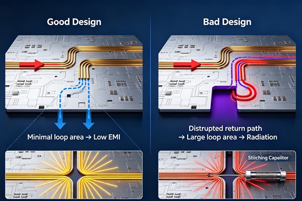
Common culprits for return path discontinuities include routing traces across splits between different power or ground domains, routing over densely packed via anti-pads (clearance holes), and changing reference layers without providing an adequate return path via for the current to follow. Learn more about Stacked vs. Staggered Microvias: Design Rules and Reliability in High-Density Interconnect (HDI) PCBs.
How to Optimize Return Paths (Step-by-Step Guide)
Follow these engineering rules.
- Identify Critical High-Speed Signals
Before routing begins, classify the nets in your schematic. Identify all high-speed digital signals (such as PCIe, DDR, USB, HDMI, and Gigabit Ethernet), clock signals, and RF traces. These critical nets are highly sensitive to return path discontinuities and must be routed with the utmost priority. Establish strict design rules regarding impedance targets and permissible layer transitions for these specific nets.
- Assign Adjacent Solid Reference Planes
Define the PCB stack-up carefully. Ensure that every signal layer designated for high-speed routing is immediately adjacent to a solid copper reference plane. A continuous ground plane is always the preferred reference because it maintains an equipotential state and does not carry DC power currents. The dielectric thickness between the signal trace and its reference plane should be minimized (typically 3 to 5 mils) to tightly couple the return current to the trace and minimize radiated emissions.
- Route Traces Without Crossing Plane Splits
The most fundamental rule of return path optimization is to never route a high-speed signal over a split or gap in the adjacent reference plane. When defining isolated ground domains or split power planes, ensure the gaps do not intersect the routing paths of critical signals. If a trace must cross a split out of absolute necessity, you must provide a tightly coupled bridge—such as a stitching capacitor placed directly adjacent to the crossing point—to allow high-frequency AC return currents to jump across the split with minimal loop area expansion.
- Provide Stitching Vias for Layer Transitions
When a high-speed trace transitions from one layer to another, the return current must also transition to the new reference plane. If the trace moves from one ground-referenced layer to another ground-referenced layer, place a ground stitching via as close as physically possible to the signal via (ideally within 40 mils). This provides a direct, low-inductance path for the return current to switch planes. If the trace transitions between a ground-referenced layer and a power-referenced layer, place an appropriately sized decoupling capacitor right next to the signal via to facilitate the return current transfer between the planes.
- Minimize Anti-Pads and Plane Voids
Through-hole components, connectors, and dense via arrays require clearance holes (anti-pads) in the internal copper planes to prevent short circuits. However, overly large or overlapping anti-pads can coalesce into massive voids, completely severing the reference plane. Carefully optimize via anti-pad dimensions to ensure that a continuous “web” of copper remains between the vias. This ensures that return currents can flow smoothly between the vias rather than being forced to detour entirely around the array.
- Verify Return Paths with Simulation Tools
Relying solely on visual inspection is insufficient for complex, high-density boards. Utilize advanced Electronic Design Automation (EDA) and 3D electromagnetic (EM) field solver tools to run Signal Integrity and Power Integrity simulations. These tools can visualize return current density, pinpoint areas of high loop inductance, and accurately predict the EMI and crosstalk resulting from subtle layout decisions. Conduct these simulations iteratively during the layout phase to catch and correct return path violations before final manufacturing.
Advanced Techniques and Considerations
While ground planes are the ideal reference, modern high-density designs often force engineers to use power planes as reference planes for some signal layers. High-frequency AC signals do not distinguish between VCC and GND; to an AC signal, a solid, low-impedance power plane looks exactly like a ground plane. However, the critical caveat is that the return current on a power plane must eventually find its way back to the source device’s ground reference. This requires an ultra-low impedance Power Distribution Network (PDN) and strategic placement of decoupling capacitors at the signal driver and receiver to stitch the AC return current from the power plane back to the ground plane.
For extremely high-frequency RF designs (e.g., mmWave radar or 5G communications), standard microstrip or stripline routing may exhibit excessive radiation or dielectric loss. In these scenarios, engineers often employ Coplanar Waveguide (CPW) routing. CPW places the signal trace and its reference ground on the same layer, tightly coupling them with a specific gap width. The top-level ground is then heavily stitched with vias to an underlying solid ground plane to ensure a robust, unbroken return path and excellent isolation from adjacent circuits.
Furthermore, consider the physical limits of the PCB fabrication process. Ensure that the copper weight of the reference planes is sufficient to handle any DC currents (if acting as a power plane) without excessive voltage drop, while maintaining extreme flatness for consistent impedance across the board profile. The meticulous alignment of stack-up layers during pressing is also vital to guarantee the precise gap between the trace and the reference plane defined in your SI models.
Conclusion
Return path optimization is not merely a recommended best practice; it is an absolute physical necessity for the reliable operation of high-frequency electronics. By internalizing the principle that high-frequency currents follow the path of least inductance, engineers can proactively design solid, unbroken reference planes. Through diligent stack-up design, careful routing strategies that avoid plane splits, and the strategic use of stitching vias and capacitors, the integrity of high-speed signals can be robustly preserved. Ultimately, a strong focus on the return path elevates a PCB design from functionally adequate to highly optimized, immune to EMI, and ready for the rigorous demands of next-generation technology.
Achieving optimal signal integrity requires a deliberate, proactive approach to reference plane design and trace routing. Follow this systematic process to optimize return paths in your high-frequency PCB designs.
Frequently Asked Questions (FAQ)
When a high-speed trace crosses a plane split, the tightly coupled return current is blocked and forced to detour around the perimeter of the split to find a continuous path back to the source. This massive increase in the current loop area sharply increases loop inductance, causing severe impedance mismatch, signal reflections, signal attenuation, and significant radiated electromagnetic interference (EMI).
Yes, high-frequency AC signals view any continuous copper plane (whether power or ground) as an adequate reference plane. However, if a signal is referenced to a power plane, the return current must eventually transition back to the system ground. This requires careful placement of high-frequency decoupling capacitors near the driver and receiver to allow the AC return current to jump between the power and ground planes without encountering high inductance.
As a general rule for high-speed digital signals, you should place at least one stitching via for every signal via when transitioning between layers referenced to the same plane net (e.g., GND to GND). The stitching via must be placed as close to the signal via as manufacturing tolerances allow (ideally within 30-40 mils) to minimize the loop inductance of the layer transition. For highly critical or differential signals, two symmetrical stitching vias are often used to provide an optimal, balanced return path.
At direct current (DC) and very low frequencies, current follows the path of least resistance. The return current spreads out across the entire reference plane and takes the shortest physical, straight-line distance back to the source. At high frequencies (generally > 100 kHz), inductive reactance dominates the impedance equation. The current follows the path of least inductance, which naturally forms directly underneath the outgoing signal trace, minimizing the loop area.
To maximize coupling and minimize loop inductance, the dielectric thickness between the signal trace and its reference plane should be as small as possible while maintaining manufacturing reliability and trace width constraints. In modern high-speed stack-ups, this distance is typically between 3 and 5 mils. Tighter coupling sharply reduces crosstalk and electromagnetic radiation.