Table of Contents
Introduction to Advanced PCBA SMT Assembly
The relentless drive toward miniaturization in electronics has pushed Printed Circuit Board Assembly (PCBA) and Surface Mount Technology (SMT) to unprecedented levels of precision. Modern consumer electronics, medical devices, and aerospace systems demand high-density interconnects, necessitating the adoption of ultra-miniature components. Among the most challenging to assemble reliably are fine-pitch Ball Grid Arrays (BGAs) and imperial 01005 (metric 0402) passive components. Learn more about AOI & 3D X-Ray: Achieving Zero-Defect PCB Assembly.
Mastering the PCBA SMT assembly process for these advanced packages is not merely a matter of upgrading equipment; it requires a holistic optimization of the entire manufacturing ecosystem. From stencil design and solder paste rheology to pick-and-place accuracy and reflow profiling, every variable must be meticulously controlled. This article provides a comprehensive B2B engineering perspective on overcoming the inherent challenges associated with fine-pitch BGA and 01005 component assembly, ensuring high yield, reliability, and performance in cutting-edge electronic assemblies.
The Engineering Challenges of Miniaturization
Fine-Pitch BGA Complexity
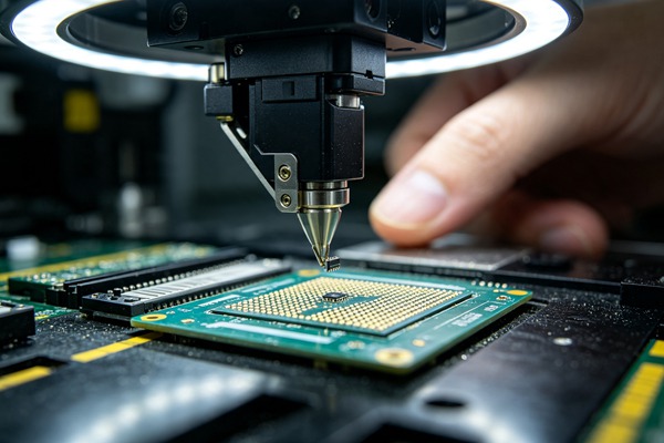
Fine-pitch BGAs (defined typically as having a ball pitch of 0.5mm or less, down to 0.3mm) offer exceptional I/O density and thermal performance. However, their physical architecture presents significant manufacturing hurdles. The primary issue is the reduced size of the solder spheres and the correspondingly small solder paste deposits required.
This reduction exacerbates the risk of defects such as:
– Head-in-Pillow (HiP): Caused by oxidation or warpage during reflow, preventing the BGA sphere from coalescing with the solder paste deposit.
– Non-Wet Opens (NWO): Similar to HiP but typically occurring on the pad side, often due to poor pad wettability or exhausted flux activity.
– Solder Bridging: Due to the close proximity of the pads, excess solder paste or placement inaccuracy can easily lead to shorts between adjacent I/O pins.
– Substrate Warpage: The mismatch in Coefficient of Thermal Expansion (CTE) between the BGA package, the PCB, and the solder joints can cause significant dynamic warpage during the reflow profile, leading to open or severely stressed joints.
01005 Component Intricacies
Imperial 01005 components measure a mere 0.4mm by 0.2mm (16 mils by 8 mils). Their microscopic size introduces a unique set of challenges that disrupt traditional SMT assembly norms.
Key challenges include:
– Tombstoning: The extreme sensitivity to surface tension imbalances during reflow can cause the component to stand on one end. This is often driven by uneven thermal mass, asymmetrical pad designs, or uneven solder paste volume.
– Component Loss: Due to their negligible mass, 01005 components are susceptible to being blown off the board by standard extraction systems or rapid airflow in the reflow oven.
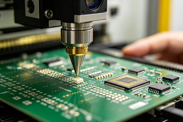
– Pick-and-Place Reliability: Vacuum nozzle design must be optimized to pick the component without damaging it, and the vision system must possess sub-micron resolution to accurately identify the component center and orientation.
– Solder Paste Release: Transfer efficiency from the stencil to the pad becomes highly critical. The Area Ratio (AR) of the stencil aperture often approaches theoretical limits, necessitating advanced stencil technologies like electroforming or nano-coatings.
Optimizing the SMT Assembly Process
To achieve high-yield assembly of these complex components, manufacturers must implement stringent process controls across the entire SMT line.
Solder Paste Printing Excellence
The foundation of successful fine-pitch BGA and 01005 assembly lies in the solder paste printing process. Industry studies suggest that up to 70% of SMT defects originate at the printer.
- Solder Paste Selection: A Type 4 or Type 5 solder paste is typically required. Type 5 paste (particle size 15-25 µm) is essential for 01005 components and 0.3mm pitch BGAs to ensure consistent release through ultra-small stencil apertures. The flux chemistry must be robust enough to survive extended preheat times without exhausting its activity, preventing HiP defects.
- Stencil Design and Technology: Step stencils may be necessary to accommodate the varying volume requirements of standard components versus fine-pitch devices. For 01005s, stencil thickness is often reduced to 2-3 mils (50-75 µm). Laser-cut stainless steel with electropolishing is the minimum standard, while nano-coated stencils significantly improve transfer efficiency and reduce the required wiping frequency.
- Printer Parameters: Closed-loop squeegee pressure control, optimized separation speed, and rigorous under-stencil wiping (using vacuum and solvent) are non-negotiable. Solder Paste Inspection (SPI) is mandatory to verify volume, area, and height in real-time, allowing for immediate process adjustments before the board reaches placement.
Precision Component Placement
The pick-and-place equipment must possess extreme accuracy and repeatability, typically requiring a Cpk > 1.33 at ±30 µm or better for 3-sigma. Learn more about Burn-in Boards (BIB): Designing High-Temperature Burn-In Boards for Semiconductor Testing.
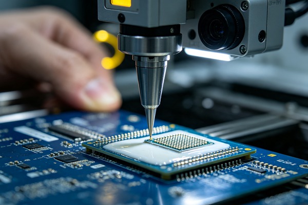
- Vision Systems: High-resolution cameras with advanced lighting algorithms are required to accurately recognize the tiny features of 01005 components and the complex ball patterns of fine-pitch BGAs.
- Nozzle Technology: Custom nozzles with compliant tips may be needed for delicate BGAs, while specialized ultra-small nozzles are required for 01005s. The vacuum flow must be carefully regulated to avoid component “tombstoning” within the nozzle itself.
- Placement Force: Real-time force feedback is critical. Excessive force can crush 01005 components or damage the internal structure of a BGA, while insufficient force can result in poor tacking to the solder paste, leading to component shift during transit to the reflow oven.
How to Assemble Fine-Pitch BGA and 01005 Components (Step-by-Step Guide)
Follow these engineering rules.
- Perform Rigorous Design for Manufacturability (DFM) Analysis
Before physical assembly begins, validate the PCB layout. Ensure pad geometries for 01005 components are symmetrical to minimize tombstoning risks. For fine-pitch BGAs, verify the escape routing, via-in-pad strategies (ensure vias are properly filled and plated over), and solder mask defined (SMD) versus non-solder mask defined (NSMD) pad configurations based on the package specifications.
- Implement Advanced Solder Paste Printing Controls
Select a high-quality Type 5, halogen-free, no-clean solder paste. Utilize a laser-cut, nano-coated stencil with a thickness optimized for the 01005 Area Ratio (typically 2 to 3 mils). Employ an automated Solder Paste Inspection (SPI) system with tight tolerance bands to monitor paste volume, height, and registration. Establish an aggressive under-stencil wipe profile to prevent aperture clogging.
- Optimize Pick-and-Place Machine Parameters
Equip your placement machines with specialized nozzles designed specifically for 01005 geometry and BGA handling. Calibrate the vision system to recognize component outlines and bump arrays with sub-pixel accuracy. Program the placement sequence to minimize Z-axis travel and optimize the placement force (typically <1.5 Newtons for 01005s) to ensure the component is embedded in the paste without being damaged.
- Develop a Characterized Reflow Profile
Use a multi-zone convection reflow oven (preferably 10+ zones) with a nitrogen atmosphere to minimize oxidation. Attach thermocouples directly to the BGA spheres (if using a sacrificial board) and near the 01005 components to accurately measure the thermal mass. Develop a linear ramp-to-spike (RTS) or a carefully controlled ramp-soak-spike (RSS) profile to minimize thermal shock, reduce substrate warpage, and ensure complete flux activation and solder coalescence.
- Execute Comprehensive Post-Reflow Inspection
Implement 3D Automated Optical Inspection (AOI) to verify component presence, polarity, and solder joint fillets for the 01005 devices. For fine-pitch BGAs, 3D AOI cannot inspect the hidden solder joints. Therefore, mandatory Automated X-ray Inspection (AXI) must be utilized to detect bridging, voiding (ensure voids are <25% of the ball area), head-in-pillow, and non-wet opens.
- Conduct Reliability and Destructive Testing
For new product introductions (NPI), perform cross-sectional analysis on sample boards to verify the intermetallic compound (IMC) thickness and joint morphology of the fine-pitch BGA and 01005 connections. Conduct dye-and-pry testing to identify any latent defects like HiP or NWO that might pass standard X-ray inspection.
Implementing a robust process requires a systematic approach. Follow these engineering guidelines to optimize your PCBA SMT assembly line for ultra-miniature devices.
Advanced Quality Assurance Techniques
The invisible nature of BGA solder joints and the microscopic size of 01005 connections demand advanced metrology and quality assurance protocols. Learn more about Embedded Components: Miniaturizing IoT Devices with Embedded PCB Components.
- 3D Automated X-Ray Inspection (AXI): Traditional 2D X-ray is insufficient for fine-pitch BGAs. 3D AXI uses laminography or computed tomography (CT) to slice the solder joint horizontally, allowing engineers to inspect the critical interface between the solder ball and the PCB pad. This is the only reliable method for detecting Head-in-Pillow and volumetric anomalies in high-density packages.
- Nitrogen Reflow Environment: While not strictly an inspection technique, utilizing a nitrogen atmosphere (oxygen levels <500 ppm) in the reflow oven drastically reduces oxidation. This significantly widens the process window for fine-pitch BGAs and improves the wetting force on the tiny pads of 01005 components, directly impacting final joint quality.
- Acoustic Microscopy (CSAM): In high-reliability applications (e.g., aerospace, automotive), Scanning Acoustic Microscopy may be employed to detect delamination within the BGA package itself or at the substrate interface, ensuring the structural integrity of the assembly after the thermal stress of reflow.
Conclusion
The integration of fine-pitch BGAs and 01005 components represents the pinnacle of modern PCBA SMT assembly. Success in this arena is not achieved through trial and error, but through a rigorous, scientifically driven engineering approach. By mastering solder paste rheology, employing state-of-the-art placement and inspection technologies, and strictly adhering to characterized thermal profiles, manufacturers can achieve the high yields and long-term reliability required by today’s advanced electronic products. As miniaturization continues to push the boundaries of physics and material science, continuous process improvement and investment in advanced manufacturing capabilities will remain paramount. Learn more about BGA Underfill: Enhancing PCBA Reliability Against Mechanical Shock and Thermal Stress.
Frequently Asked Questions (FAQ)
Tombstoning in 01005 components is primarily caused by an imbalance in surface tension forces during the reflow process. This imbalance can result from asymmetrical pad design, uneven solder paste volume, thermal mass differentials between the two pads, or heating rates that cause the paste on one pad to melt faster than the other.
Type 5 solder paste utilizes smaller solder particles (typically 15-25 µm in diameter) compared to the standard Type 3 or Type 4 pastes. These smaller particles are essential for achieving consistent paste release through the exceptionally small stencil apertures required for 01005 pads and sub-0.5mm pitch BGAs, ensuring adequate volume and reducing the risk of clogging.
Head-in-Pillow (HiP) defects are notorious because they often maintain electrical contact under ambient conditions but fail under stress or thermal cycling. Standard 2D X-ray struggles to detect them. The most reliable non-destructive method for detecting HiP is 3D Automated X-Ray Inspection (AXI) or CT scanning, which can visualize the lack of coalescence at the pad interface. Destructive testing like dye-and-pry is also used for process validation.
While 01005 components can technically be reflowed in an air atmosphere, a nitrogen environment (low oxygen concentration) is highly recommended. Nitrogen significantly reduces the oxidation of the small solder powder particles and the component metallization. This improves the wetting action, increases the process window, and significantly reduces the incidence of defects like tombstoning and non-wet opens.
The Area Ratio (AR) is the ratio of the area of the stencil aperture opening to the area of the aperture walls. For reliable solder paste release, an AR of >0.66 is traditionally recommended. However, with the extreme miniaturization of 01005s, engineers often have to push this limit. Using advanced nano-coated electroformed stencils, acceptable printing can sometimes be achieved with an AR closer to 0.55, though it requires meticulous process control.