Table of Contents
Introduction to High-Temperature Burn-In Testing
In the rigorous world of semiconductor manufacturing and reliability engineering, burn-in testing represents a critical phase designed to ensure device longevity and prevent catastrophic field failures. By subjecting integrated circuits (ICs) and discrete semiconductors to elevated temperatures and dynamic electrical bias over an extended duration, burn-in testing effectively accelerates the aging process. This accelerated life testing is engineered to weed out “infant mortality” failures—devices with latent manufacturing defects that would otherwise fail early in their operational lifespan. Learn more about Press-Fit Connectors: PCB Manufacturing Tolerances for Solderless Interconnects.
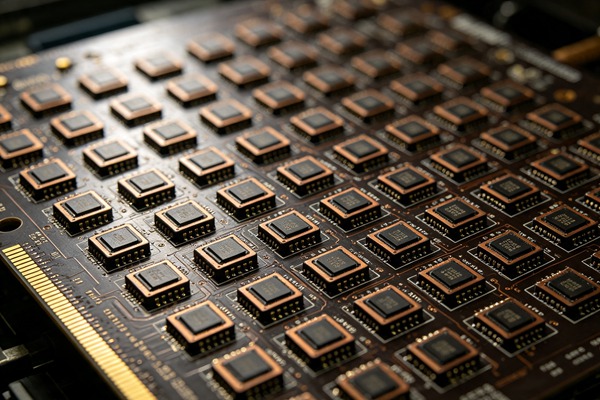
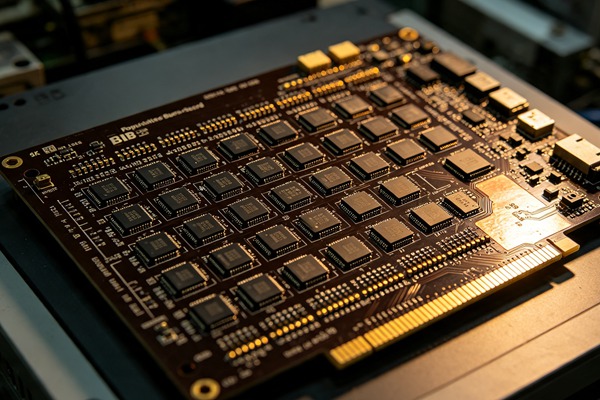
As modern electronics penetrate more demanding sectors—such as aerospace, defense, downhole drilling, and automotive applications like Electric Vehicles (EVs)—the environmental baseline for these components has dramatically increased. Standard silicon components are being pushed to their limits, while wide-bandgap (WBG) semiconductors like Silicon Carbide (SiC) and Gallium Nitride (GaN) are designed specifically to operate in extreme environments. Consequently, the test infrastructure must evolve. Central to this infrastructure is the Burn-In Board (BIB), a specialized printed circuit board engineered to interface dozens or hundreds of Devices Under Test (DUT) with the testing stimulus, all while resting inside a high-temperature burn-in oven.
Designing a high-temperature BIB is an exercise in extreme environmental engineering. A standard printed circuit board is designed to operate comfortably in ambient conditions, perhaps reaching 85°C to 105°C under heavy load. In contrast, a high-temperature BIB must endure continuous exposure to environments ranging from 125°C to well over 250°C for thousands of hours. It must survive these conditions while maintaining flawless signal integrity, structural stability, and reliable power delivery, acting as a flawless conduit between the test equipment and the semiconductor being evaluated. Learn more about Sequential Lamination: Mastering the Manufacturing Process for Any-Layer HDI Boards.
Key Engineering Challenges in High-Temperature BIB Design
The design of a high-temperature Burn-In Board presents a multifaceted engineering challenge, requiring a delicate balance between mechanical resilience, thermal management, and electrical performance.
Thermal Mechanical Stress and Fatigue
The most pervasive enemy of a high-temperature BIB is thermal mechanical stress. As the board cycles from room temperature ambient up to extreme burn-in temperatures and back down again, the various materials comprising the board expand and contract. Because the PCB substrate, the copper traces, the plated through-holes (PTH), and the heavy test sockets all possess vastly different Coefficients of Thermal Expansion (CTE), significant mechanical strain is induced at their interfaces. Over hundreds of thermal cycles, this sheer stress can cause micro-cracking in the vias, pad lifting, and delamination of the internal layers. Engineering around CTE mismatch is fundamental to ensuring the board outlasts the components it is designed to test.
Oxidation and Material Degradation
At elevated temperatures, chemical reactions accelerate exponentially. Standard PCB surface finishes and exposed copper will oxidize rapidly, leading to a drastic increase in contact resistance. This oxidation can corrupt test signals, induce localized heating, and eventually cause open circuits. Furthermore, the base resin of the PCB substrate can begin to outgas, lose mass, or suffer a breakdown in its dielectric properties, completely altering the impedance profile of the board and potentially contaminating the burn-in chamber.
Maintaining Power and Signal Integrity (PI/SI)
Power delivery across a massive burn-in board is notoriously difficult at high temperatures. Copper possesses a positive temperature coefficient of resistance; as it gets hot, its electrical resistance increases. When distributing high currents across a board populated with numerous active DUTs, this increased resistance leads to substantial I-R voltage drops. If not properly compensated for with excessively wide traces and heavy copper weights, the ICs farthest from the edge connector may suffer from voltage starvation or severe ground bounce. Additionally, the dielectric constant (Dk) and dissipation factor (Df) of the substrate materials will shift at high temperatures, complicating the routing of high-speed dynamic stimulus signals and clock lines.
Material Selection for Extreme Environments
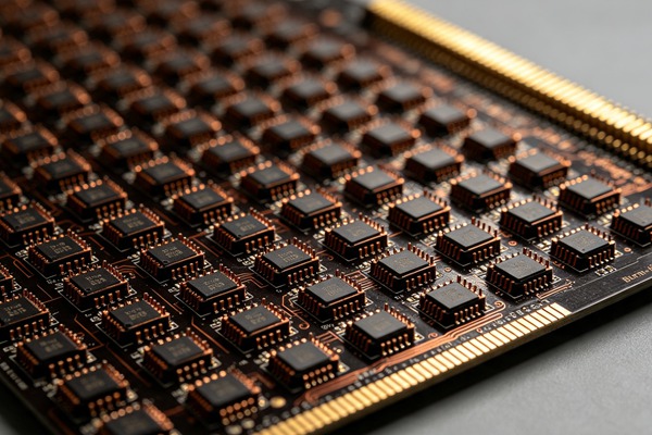
The foundation of a robust, high-temperature BIB is the selection of advanced materials capable of surviving the oven environment without compromising electrical performance. Standard FR-4, widely used in consumer electronics, is categorically inadequate for sustained high-temperature burn-in. Its Glass Transition Temperature (Tg)—the point at which the polymer matrix transitions from a rigid, glassy state to a soft, rubbery state—typically maxes out around 130°C to 150°C. Operating at or above the Tg causes massive Z-axis expansion, instantly rupturing vias. Learn more about Backdrilling: Eliminating Signal Reflection with Precise Controlled Depth Backdrilling.
Advanced Substrates: Polyimide and Ceramics
For high-temperature applications up to 200°C, high-Tg Polyimide is the undisputed industry standard. Polyimide laminates maintain excellent mechanical stability, tensile strength, and consistent dielectric properties at temperatures that would destroy FR-4. Crucially, polyimide exhibits a highly stable and relatively low Z-axis CTE even at elevated temperatures, drastically reducing the strain on plated through-holes during thermal cycling.
When testing wide-bandgap semiconductors at ultra-high temperatures exceeding 200°C and pushing toward 250°C or 300°C, engineers must abandon organic resins entirely and pivot to advanced inorganic materials. Ceramic substrates, such as Alumina (Al2O3) or Aluminum Nitride (AlN), are frequently employed. While these materials offer unparalleled thermal stability and high thermal conductivity, they are brittle, expensive, and require specialized manufacturing processes, making layout density a significant challenge.
High-Reliability Surface Finishes
To combat rapid oxidation, the surface finish of a high-temperature BIB must be exceptionally durable. Standard HASL (Hot Air Solder Leveling) and OSP (Organic Solderability Preservative) are not viable. Instead, designers rely on heavy gold plating. Electroless Nickel Immersion Gold (ENIG) provides a good baseline, but for areas subject to mechanical wear—specifically the socket contact pads and the board edge connectors—Hard Gold plating is mandatory. Hard gold alloys provide superior wear resistance against repeated insertions and exceptional oxidation resistance, ensuring that contact resistance remains negligible over the board’s lifespan.
Test Sockets and On-Board Components
A Burn-In Board is highly dependent on its electromechanical interfaces. The test sockets that cradle the DUTs are subjected to the highest concentration of thermal and mechanical stress.
High-temperature sockets must be precision-machined or injection-molded from advanced engineering thermoplastics. Materials like PEEK (Polyetheretherketone) or Torlon (Polyamide-imide) are highly favored for their ability to maintain dimensional stability, resist creeping, and offer excellent insulative properties at temperatures approaching 250°C. The internal contact pins are typically formed from Beryllium Copper (BeCu) alloys, which retain their spring force and mechanical resilience at high heat. These pins are heavily gold-plated to ensure a low-resistance path between the board and the device.
Similarly, any passive components required on the board—such as decoupling capacitors, pull-up resistors, or protection diodes—must be strictly rated for the ambient oven temperature. Commercial-grade components will fail precipitously. Designers must specify automotive (AEC-Q200 Grade 0) or military-grade high-temperature passives, ensuring that the encapsulants and internal structures of these components will not degrade or outgas under continuous thermal load.
How to Design a High-Temperature Burn-In Board (Step-by-Step Guide)
Follow these engineering rules.
- Define Test Parameters and Environmental Constraints
The design process begins with a rigorous specification phase. Engineers must establish the absolute maximum burn-in temperature, the anticipated thermal cycling profile (ramp rates and dwell times), and the required lifespan of the board (e.g., thousands of hours or specific number of insertion cycles). Simultaneously, the electrical load must be defined: maximum current draw per DUT, total power dissipation for the fully populated board, and the frequency requirements for the dynamic signal stimulus.
- Select the Appropriate Substrate Material
Based on the thermal parameters defined in the first step, select a PCB substrate that offers an appropriate Glass Transition Temperature (Tg) and Decomposition Temperature (Td). For continuous operation up to 200°C, specify a high-Tg Polyimide laminate. If the application exceeds 200°C, collaborate with fabricators to utilize advanced ceramic substrates or specialized high-temperature Teflon-based laminates.
- Choose High-Temperature Sockets and Connectors
Work directly with specialized socket vendors to select or custom-design test sockets that match the DUT package and the target temperature range. Ensure that the socket body material (e.g., PEEK) and contact pin metallurgy (e.g., Gold-plated BeCu) are certified for the operational envelope. Specify heavy Hard Gold plating for the edge connector fingers that interface with the oven driver boards to guarantee long-term reliable mating.
- Perform Thermal and Mechanical Simulation
Prior to detailed routing, perform thermal-electrical co-simulation. A fully loaded BIB can dissipate substantial localized heat. Model the thermal mass of the sockets, the heat generated by the DUTs, and the ambient airflow within the burn-in oven. Adjust the component placement to prevent the creation of thermal hotspots. Ensure sufficient spacing between DUTs to allow convective cooling to maintain uniform temperatures across all devices.
- Route Traces for Signal Integrity and Power Distribution
Execute the PCB layout with a strong emphasis on robust power delivery. Because copper resistance increases with heat, utilize ultra-wide traces, heavy copper weights (2 oz or 3 oz), and massive internal power and ground planes to minimize I-R voltage drops. When routing high-speed dynamic signals, calculate impedance profiles using the substrate’s high-temperature Dk/Df values, not standard room temperature specifications. Implement mechanical reliability techniques such as teardrops on all vias and pads to prevent trace fracturing during thermal cycling.
- Finalize Verification and Fabrication
Subject the completed layout to rigorous Design Rule Checks (DRC) tailored for high-temperature manufacturing. Verify every line item on the Bill of Materials (BOM) to guarantee that all solder masks, surface finishes, passives, and substrate materials are explicitly rated for the extreme environment. Finally, partner with a specialized PCB manufacturer that possesses a proven track record in high-reliability, polyimide, or ceramic board fabrication, as these processes require strict environmental controls and curing cycles entirely different from standard FR-4 production.
Designing a reliable BIB requires a systematic approach, heavily front-loaded with mechanical and thermal considerations before the first electrical trace is routed.
The Economics and ROI of High-Quality BIBs
Investing in meticulously engineered, high-temperature burn-in boards carries a significant upfront cost. Advanced materials like polyimide, precision PEEK sockets, and heavy hard gold plating are expensive. However, in the context of high-reliability semiconductor manufacturing, this investment yields a profound Return on Investment (ROI). Learn more about Ceramic PCBs: Alumina vs. Aluminum Nitride (AlN) Ceramic PCBs for Extreme Heat.
A poorly designed BIB using marginal materials will fail prematurely, resulting in aborted burn-in runs, false failures (where the board fails, not the DUT), and potentially the destruction of highly expensive semiconductor batches. Furthermore, inaccurate test results caused by signal degradation or voltage drops can lead to defective components slipping into the supply chain, culminating in catastrophic field failures, massive recall costs, and irreversible brand damage. A heavily engineered high-temperature BIB ensures continuous, reliable throughput in the testing facility, acting as a critical safeguard for the semiconductor manufacturer’s bottom line and reputation.
Frequently Asked Questions (FAQ)
Standard burn-in testing typically occurs between 125°C and 150°C. However, for specialized components designed for aerospace, defense, downhole drilling, or wide-bandgap (SiC/GaN) automotive applications, high-temperature burn-in environments frequently range from 175°C to well over 250°C.
Standard FR4 has a Glass Transition Temperature (Tg) of approximately 130°C to 150°C. When exposed to temperatures near or above this threshold for extended periods, FR4 becomes structurally soft, warps, and experiences dramatic Z-axis thermal expansion. This rapid expansion causes the plated through-holes (PTH) to fracture, leading to immediate electrical failure and board destruction.
High temperatures significantly increase the DC resistance of copper traces. This causes larger voltage drops across the power distribution network, potentially starving the devices under test of necessary voltage. Additionally, exposed copper oxidizes rapidly under extreme heat, which is why heavy gold plating is critical to protect contact points and preserve signal integrity.
Burn-in testing accelerates the natural aging process of semiconductor devices by subjecting them to extreme thermal and electrical stress. Its primary role is to precipitate early-life failures (known as infant mortality) caused by latent manufacturing defects. This ensures that only highly reliable components are shipped and deployed in mission-critical applications.
High-temperature test sockets are typically machined or molded from advanced engineering thermoplastics like PEEK (Polyetheretherketone) or Torlon. The internal spring contacts are usually made from resilient alloys such as Beryllium Copper (BeCu) and are heavily plated with gold to maintain reliable electrical connection and mechanical force despite the extreme heat.