Table of Contents
Introduction to PCB Backdrilling and Signal Integrity
In the realm of high-speed Printed Circuit Board (PCB) engineering, maintaining pristine signal integrity is paramount. As data transfer rates escalate into the multi-gigabit per second range, even minor physical imperfections in the interconnect structures can lead to significant signal degradation. One of the primary culprits in these high-speed designs is the presence of via stubs—unnecessary sections of plated through-holes (PTH) that extend beyond the required signal layers.
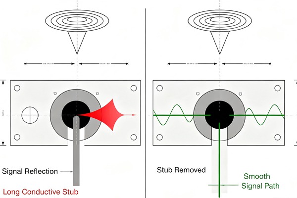
When high-speed signals encounter these via stubs, the electrical energy is partially reflected back toward the source, causing constructive and destructive interference. This phenomenon, known as signal reflection, degrades the eye diagram, increases the bit error rate (BER), and can ultimately lead to system failure. To combat this, PCB engineers employ a highly effective technique known as backdrilling, or controlled depth backdrilling.
Backdrilling systematically removes these extraneous via stubs, optimizing the transmission line characteristics of the vias and ensuring that high-speed signals propagate without detrimental reflections.
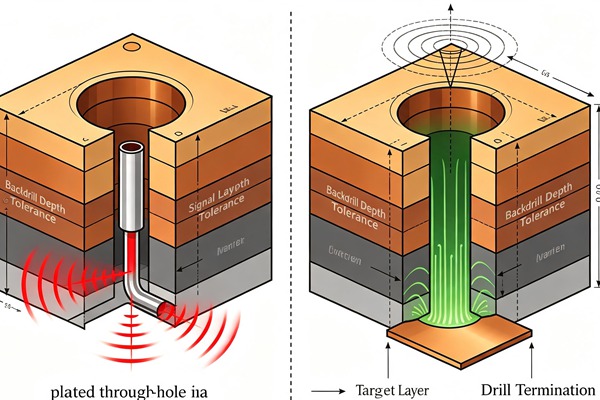
The Mechanics of Signal Reflection from Via Stubs
To fully appreciate the necessity of controlled depth backdrilling, it is critical to understand the physics of via stubs and signal reflection. A via acts as a transmission line transitioning between different layers of a PCB. When a via connects, for instance, layer 1 to layer 3 in a 12-layer board, the remaining plated barrel from layer 3 down to layer 12 is electrically superfluous. This unused portion is the via stub.
From a microwave engineering perspective, this stub behaves as an unterminated transmission line. When a high-frequency signal propagates through the active portion of the via and reaches the junction of the stub, a portion of the electromagnetic wave continues down the stub. Because the end of the stub is an open circuit, the wave reflects perfectly and travels back up the stub. Learn more about Conformal Coating: Protecting PCBA from Moisture, Dust, and Corrosive Environments.
When the reflected wave recombines with the primary signal, it causes interference. If the length of the stub approaches a quarter of the wavelength of the signal’s highest frequency component, the stub acts as a notch filter, severely attenuating that frequency. This results in signal distortion, increased jitter, and reduced operational margins. Eliminating this resonant structure is precisely what backdrilling achieves. Learn more about Ceramic PCBs: Alumina vs. Aluminum Nitride (AlN) Ceramic PCBs for Extreme Heat.
Advantages of Precise Controlled Depth Backdrilling
Implementing controlled depth backdrilling in high-speed PCB fabrication offers profound advantages that directly impact the performance and reliability of the final electronic product.
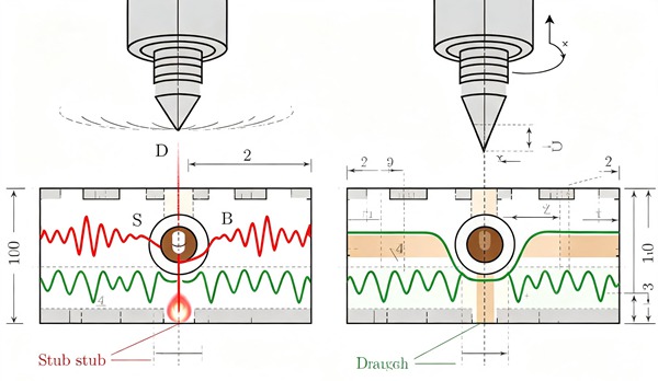
Firstly, backdrilling dramatically reduces deterministic jitter. By removing the physical structure responsible for multi-path propagation and resonant reflections, the signal arrives at the receiver with significantly lower phase noise and timing uncertainty. This allows communication links to operate flawlessly at higher data rates.
Secondly, backdrilling minimizes signal attenuation. The energy that would otherwise be lost into the via stub and reflected out of phase is instead preserved within the primary signal path. This improves the overall insertion loss characteristics of the channel, enabling longer trace runs or the use of more cost-effective dielectric materials while still meeting the loss budget.
Furthermore, removing via stubs decreases electromagnetic interference (EMI) and cross-talk. Stubs can act as radiating antennas, coupling energy into adjacent traces or planes. By physically removing the stub, backdrilling reduces the parasitic capacitance and inductance of the via structure, tightly confining the electromagnetic fields and mitigating crosstalk in dense, high-speed routing areas.
Design Considerations for Backdrilled PCBs
Integrating backdrilling into a PCB design requires careful planning and coordination with the fabrication facility. Engineers must account for several critical design parameters to ensure successful execution.
Identifying Critical Nets: Not all vias require backdrilling. The process adds manufacturing cost and complexity, so it should be reserved for high-speed nets where stub length will demonstrably impact signal integrity. Typically, differential pairs operating above 3 Gbps (such as PCIe Gen 3/4/5, 10G/40G/100G Ethernet, and DDR4/DDR5) are prime candidates.
Clearance and Keep-Out Zones: The backdrilling process utilizes a drill bit slightly larger than the original via drill to remove the plating. Consequently, designers must define larger anti-pads (clearance holes in the power and ground planes) on the layers being drilled through. Trace routing must also avoid these enlarged keep-out zones to prevent accidental severing of adjacent traces during the backdrilling operation.
Stub Length Tolerance: Absolute removal of the entire stub is physically impossible without risking damage to the internal layer connection. Manufacturers specify a minimum remaining stub length and a tolerance (typically around +/- 5 to 10 mils). Engineers must run pre-layout signal integrity simulations using these tolerance values to confirm that the maximum allowable remaining stub will not cause unacceptable reflections.
Layer Stackup Optimization: The layer stackup should be designed with backdrilling in mind. Grouping high-speed signals on adjacent layers or routing them closer to the primary component side can minimize the required depth of the backdrill, simplifying the manufacturing process and reducing costs.
How to Implement Backdrilling in Your PCB Design (Step-by-Step Guide)
Follow these engineering rules. Learn more about Skew Compensation: Managing Fiber Weave Effect (FWE) and Length Matching for PCIe Gen 6.
- Perform Pre-Layout Signal Integrity Analysis
Begin by determining the maximum allowable stub length for your specific high-speed protocols. Use 3D electromagnetic solvers or signal integrity simulation tools to model the channel. Sweep the via stub length to identify the point at which return loss and insertion loss specifications are violated. This analysis establishes the baseline requirements for your backdrilling constraints.
- Define Backdrill Specifications in the EDA Tool
Modern Electronic Design Automation (EDA) tools offer specific features for managing backdrilling. Open your constraint manager and define which nets or via structures require backdrilling. Specify the start layer (the surface layer from which the drill enters) and the stop layer (the internal layer where the trace connects).
- Adjust Anti-Pads and Clearance Rules
Configure the Design Rule Check (DRC) engine to accommodate the larger drill bits used in backdrilling. Increase the anti-pad diameters on the plane layers that the backdrill will pass through. Ensure that trace-to-via clearance rules are updated to prevent routing too close to the backdrilled holes, accounting for drill wander tolerances.
- Route High-Speed Nets and Add Vias
Proceed with routing your high-speed differential pairs and critical signals. As you place vias to transition between layers, the EDA tool should automatically recognize the backdrill requirements based on your constraints and apply the necessary clearance rules. Optimize your routing to minimize the number of layer transitions whenever possible.
- Generate Backdrill Fabrication Data
Once routing is complete and DRCs are clean, generate the manufacturing files. You must produce separate NC drill files specifically for the backdrilling operations. These files instruct the fabricator exactly where to drill, from which side of the board, and the precise controlled depth required to reach just above the stop layer without severing the connection.
- Communicate clearly with the PCB Manufacturer
Do not rely solely on the fabrication files. Provide a comprehensive fabrication drawing that explicitly details the backdrilling requirements. Include a stackup diagram indicating the start and stop layers, the required remaining stub length, the backdrill bit sizes, and any specific testing requirements, such as Time Domain Reflectometry (TDR) measurements, to verify the impedance and stub removal.
The successful implementation of controlled depth backdrilling involves a systematic approach from initial design through to manufacturing data generation. Follow these steps to ensure precision and reliability.
The Manufacturing Process of Controlled Depth Backdrilling
The actual fabrication of a backdrilled PCB requires specialized equipment and tight process controls. The process begins after the standard through-hole plating is complete.
First, the PCB is mounted on a highly precise, computer numerical control (CNC) drilling machine equipped with a specialized depth-sensing system. Because the thickness of a PCB can vary slightly across its surface due to lamination tolerances, simply drilling to a fixed Z-axis coordinate is insufficient.
To achieve controlled depth, the drill machine utilizes a conductive mapping technique or a laser sensor. The machine touches down on the surface of the copper pad to establish a local zero reference point for each specific via location.
Once the surface reference is established, the machine drills down into the via barrel using a bit typically 4 to 8 mils larger than the primary drill bit. The drill proceeds to the exact calculated depth—stopping a few mils short of the internal signal layer to leave a safe, minimal stub and prevent damaging the trace connection. Learn more about Burn-in Boards (BIB): Designing High-Temperature Burn-In Boards for Semiconductor Testing.
After drilling, the board undergoes a high-pressure cleaning process to remove any copper shavings or debris left inside the hole, which could cause shorts. The backdrilled holes may be left bare or filled with a non-conductive epoxy to prevent chemical entrapment during subsequent assembly processes.
Advanced Alternatives to Backdrilling
While backdrilling is a highly effective and widely used technique, there are alternative methods for eliminating via stubs, each with its own advantages and cost implications.
Blind and Buried Vias: Using High-Density Interconnect (HDI) technology with blind vias (connecting a surface layer to an internal layer without penetrating the whole board) and buried vias (connecting internal layers only) inherently eliminates stubs. However, sequential lamination cycles significantly increase manufacturing costs compared to standard through-hole boards with backdrilling.
E-Glass and Low-Loss Laminates: While not a replacement for stub removal, utilizing advanced dielectric materials with lower dissipation factors (Df) and tighter glass weaves can mitigate the overall channel loss, potentially providing enough margin that a short stub becomes acceptable.
Alternative Routing Strategies: In some cases, careful layer stackup planning allows engineers to route high-speed signals only on the outermost layers or utilize the full depth of the via (e.g., routing from Top to Bottom layer), naturally resulting in a zero-stub via structure.
Ultimately, the choice between backdrilling and HDI technologies is a trade-off between electrical performance requirements, board density, and overall manufacturing budget. For many high-speed applications, controlled depth backdrilling remains the most cost-effective compromise for achieving excellent signal integrity.
Frequently Asked Questions (FAQ)
Most high-quality PCB manufacturers can maintain a depth tolerance of +/- 5 mils (0.127 mm), leaving a minimum safe stub length of approximately 5 to 10 mils to ensure the internal connection is not damaged.
Yes, backdrilling adds cost because it requires a secondary drilling operation, specialized depth-sensing drill machines, additional programming time, and extra cleaning steps. However, it is generally much less expensive than moving to an HDI stackup with sequential laminations.
Yes, it is common to backdrill vias from both the top and bottom sides of the PCB if high-speed signals are routed on middle layers. Each backdrill operation will require its own set of NC drill files and specifications.
The most effective way to verify backdrilling is through Time Domain Reflectometry (TDR) testing on coupons or actual traces, which can clearly show the impedance profile and the absence of the capacitive drop associated with a long via stub. Additionally, cross-sectioning (microsectioning) sample vias allows for visual inspection and precise measurement of the remaining stub length.
No, backdrilling should only be applied to the specific vias carrying high-speed signals where the stub length is a significant fraction of the signal wavelength. Applying it to low-speed signals, power, or ground vias adds unnecessary cost without providing any functional benefit.