Table of Contents
Introduction to Glass Substrates in Advanced Packaging
For decades, the semiconductor and printed circuit board (PCB) industries have relied heavily on organic substrates—such as FR-4 and bismaleimide triazine (BT) epoxy—and silicon interposers to bridge the critical gap between integrated circuits (ICs) and the motherboard. However, as the global demand for high-performance computing (HPC), artificial intelligence (AI), 5G/6G telecommunications, and advanced driver-assistance systems (ADAS) accelerates exponentially, these traditional materials are rapidly reaching their physical, thermal, and electrical limits. Enter glass substrates.
Glass substrates in PCB manufacturing and advanced IC packaging represent a massive paradigm shift in how the industry manages the intricate demands of next-generation microelectronics. Offering superior dimensional stability, exceptional thermal properties, and unmatched high-frequency performance, glass is poised to become the foundational material for the future of high-density interconnect (HDI) and heterogeneous integration. This transition is not merely an incremental upgrade or a minor process tweak; it is a fundamental redesign necessary to sustain Moore’s Law and enable the massively complex chiplet-based architectures of tomorrow.
The Physical and Electrical Imperative for Glass
The relentless push toward sub-nanometer semiconductor nodes and the assembly of massive, multi-die packages highlight the inherent shortcomings of traditional organic materials. Organic substrates predictably suffer from severe warpage due to significantly mismatched coefficients of thermal expansion (CTE) between the rigid silicon die and the pliable substrate. This warpage complicates the assembly process, leads to premature solder joint failures, and strictly limits the maximum viable size of the package. Silicon interposers, while excellent for ultra-fine-pitch interconnects, are cost-prohibitive for large-scale applications and are ultimately constrained by the physical size limitations of standard silicon wafers (the reticle limit).
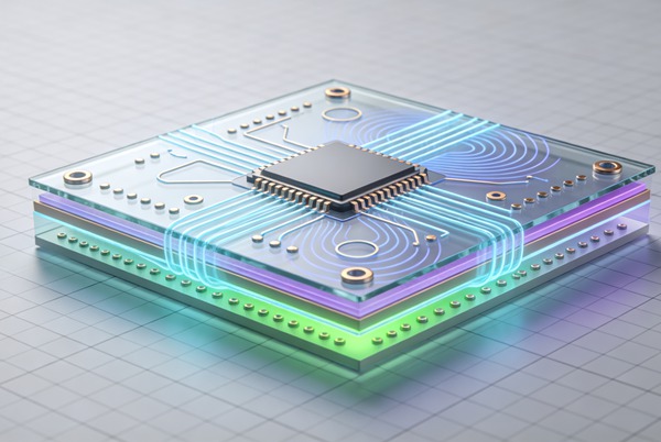
Glass, specifically engineered borosilicate and proprietary alkali-free aluminosilicate variants, offers a compelling and technologically elegant middle ground. It delivers properties that outclass both organic and silicon alternatives in specific critical engineering areas.
Exceptional Dimensional Stability and Flatness
One of the most significant and immediate advantages of glass is its mechanical rigidity and ultra-flat surface profile. Glass substrates can be manufactured with extremely low surface roughness (Ra < 1 nm). This near-perfect flatness is absolutely essential for reliably defining ultra-fine line and space (L/S) routing down to sub-2 µm dimensions using advanced lithography. Furthermore, the CTE of glass can be precisely tuned during the manufacturing process to closely match that of silicon (approximately 3.2 ppm/°C). This CTE matching drastically reduces thermally induced warpage during the high-temperature solder reflow process, enabling the fabrication of massive package sizes (e.g., 100 mm x 100 mm, 120 mm x 120 mm, and beyond) that would be physically impossible to yield with organic substrates.
Superior High-Frequency Performance
In high-speed data transmission environments (above 100 Gbps, moving towards 224 Gbps per lane) and high-frequency RF applications (such as 5G mmWave and 77 GHz automotive radar), maintaining pristine signal integrity is paramount. Glass exhibits a profoundly low dielectric constant (Dk) and an ultra-low dissipation factor (Df). Unlike organic materials, which can absorb ambient moisture and degrade signal quality over time, glass is completely hermetic. Its dielectric properties remain exceptionally stable across broad temperature and humidity ranges. This results in significantly lower insertion loss, reduced cross-talk, and minimal signal dispersion, making it an ideal, pristine dielectric medium for high-frequency IC packaging and high-speed data routing.
Through-Glass Via (TGV) Technology: The Core Enabler
The true technological enabler of glass substrates is the Through-Glass Via (TGV). Conceptually similar to Through-Silicon Vias (TSVs), TGVs provide critical vertical electrical connections through the substrate, allowing for 3D stacking and high-density routing. However, TGVs offer distinct performance advantages. Because glass is inherently a perfect electrical insulator, TGVs do not require the thick, complex isolation oxide layers needed for TSVs (which are required to prevent signal leakage into the semiconducting silicon substrate). This intrinsic insulation inherently reduces parasitic capacitance and allows for significantly tighter TGV pitches. Advanced manufacturing techniques, particularly Laser-Induced Deep Etching (LIDE) and electrical discharge machining processes, can now produce highly uniform, high-aspect-ratio TGVs at scale, facilitating unprecedented vertical via densities without compromising the substrate’s structural integrity. Learn more about Under-Stencil Cleaning: Best Practices for Fine-Pitch SMT Printing.
The Role of Glass in Heterogeneous Integration and Chiplets
The semiconductor industry is shifting rapidly from massive, monolithic system-on-chip (SoC) designs to heterogeneous integration utilizing chiplets. This advanced approach involves breaking down a large, complex die into smaller, specialized functional blocks (chiplets)—each fabricated on its most optimal, cost-effective process node—and then packaging them closely together to function as a single logical unit.
Glass substrates are uniquely positioned to support and accelerate this architecture. The ultra-fine line routing enabled by the flat glass surface allows for extremely dense die-to-die (D2D) interconnects, rivaling the bandwidth densities previously only achievable with expensive 2.5D silicon interposers (such as TSMC’s CoWoS technology). Furthermore, glass allows for the seamless integration of passive components—such as high-Q inductors, specialized capacitors, and resistors—directly into the substrate itself. This integrated passive device (IPD) capability frees up highly valuable board real estate, significantly reduces parasitic losses associated with surface-mounted discrete components, and drastically improves overall power delivery network (PDN) efficiency and signal integrity.
Implications for 5G, 6G, and Future Telecommunications
The telecommunications sector stands to benefit immensely from the widespread adoption of glass substrates. As 5G networks mature and shift heavily into the millimeter-wave (mmWave) spectrum, and as research into sub-Terahertz 6G applications accelerates, the material properties of the PCB and packaging become a primary limiting factor. Organic substrates introduce unacceptable levels of signal attenuation at these extreme frequencies. Learn more about Flex PCB Stiffeners: Choosing Between FR4, Polyimide, and Stainless Steel.
Glass, with its near-zero moisture absorption and remarkably flat dielectric response across vast frequency bands, allows antenna-in-package (AiP) designs to operate with significantly higher efficiency and lower power consumption. RF modules built on glass substrates can achieve tighter antenna arrays, better beamforming accuracy, and lower thermal dissipation, making them essential for the next generation of base stations, mobile devices, and satellite communication links.
Challenges in Glass Substrate Commercialization
Despite the profound and well-documented benefits, the broad industry transition to glass substrates in PCB and IC packaging is not without significant engineering challenges that materials scientists and manufacturing engineers are actively working to solve.
Handling and Brittleness
Glass is inherently brittle and prone to catastrophic failure from micro-fractures. The automated handling of large, ultra-thin (down to 100 µm or less) glass panels during the complex series of lithography, plating, and etching steps requires highly specialized equipment. Any micro-cracks introduced during panel edge cutting, laser routing, or via drilling can propagate rapidly under thermal stress and lead to panel breakage. Manufacturers are developing advanced edge-healing techniques (using specialized lasers to melt and seal micro-cracks), temporary bonding to rigid carriers, and novel aerodynamic transport mechanisms to mitigate these handling risks.
Metallization Adhesion
Achieving robust, long-term adhesion of copper plating to a perfectly smooth, non-porous glass surface is remarkably difficult. Unlike organic substrates, where chemical desmearing creates a micro-roughened surface for mechanical interlocking of the copper, glass requires sophisticated, atomic-level adhesion promoters. Current state-of-the-art techniques involve depositing ultra-thin titanium, chromium, or tantalum seed layers via physical vapor deposition (PVD) or utilizing advanced silane-based chemical coupling agents before copper electroplating. Ensuring this critical interface survives rigorous thermal cycling and shock testing without delamination is paramount for long-term field reliability.
Thermal Management
While glass is an excellent electrical insulator, it is a relatively poor thermal conductor compared to silicon or specialized metal-core organic substrates. In high-power HPC and AI applications, extracting hundreds of watts of heat from a dense cluster of chiplets through the glass substrate poses a formidable engineering challenge. Engineers are actively addressing this by designing dense arrays of thermal-only TGVs (solid copper-filled vias specifically placed to act as thermal conduits rather than electrical pathways), utilizing advanced thermal interface materials (TIMs), and implementing aggressive direct-to-die liquid cooling solutions that bypass the substrate entirely for primary heat dissipation.
How to Transition to Glass Substrate Prototyping (Step-by-Step Guide)
Follow these engineering rules.
- Define High-Frequency and Thermal Requirements
Begin by exhaustively profiling your system’s exact requirements. Identify the specific signal integrity bottlenecks (e.g., maximum allowable insertion loss at 112G or 224G PAM4) and the absolute thermal dissipation requirements of your chiplet architecture. Determine if a precise, tunable CTE glass variant is strictly necessary to mitigate warpage for your target physical package size.
- Select the Appropriate Glass Material Formulation
Work intimately with leading glass material suppliers to select the right substrate formulation. Standard borosilicate glass is common for general advanced packaging, while specialized fused silica or highly proprietary alkali-free aluminosilicate formulations may be absolutely required for ultra-low Dk/Df high-frequency applications or specific, highly constrained CTE matching targets.
- Design for TGV (Through-Glass Via) Integration
Adapt and rewrite your PCB/substrate design rules specifically for TGVs. Unlike standard mechanical drilling in FR-4, TGV design rules depend heavily on the specific via formation process (e.g., laser-assisted etching vs. electrical discharge). Precisely define your required aspect ratios, minimum via pitch, and metallization fill requirements (conformal plating vs. fully solid filled vias). Keep strict parasitic capacitance models in mind during the physical layout phase.
- Optimize Metallization and Adhesion Layers
Collaborate deeply with your substrate manufacturing partner to define the exact metallization stack. Because copper fundamentally repels bare glass, specify the exact sputtering or chemical vapor deposition (CVD) process for the titanium/copper (Ti/Cu) or chromium/copper (Cr/Cu) seed layer. Ensure that the chosen adhesion layer metal does not negatively impact the high-frequency skin effect for your critical RF signals.
- Execute Small-Batch Prototyping and Reliability Testing
Do not attempt to immediately scale to mass production. Utilize highly specialized advanced packaging foundries to produce controlled, small-batch prototypes. Subject these prototypes to rigorous reliability testing, focusing specifically on extreme thermal cycling (to test for CTE mismatch stress and metal delamination) and Highly Accelerated Stress Testing (HAST) to rigorously ensure the long-term hermeticity of the TGVs and the absolute stability of the dielectric properties over simulated decades of use.
Integrating glass into your high-frequency packaging roadmap requires careful strategic planning and close collaboration with specialized foundries and materials suppliers. Here is a high-level guide on how engineering teams can begin this critical transition. Learn more about Solder Voiding under QFN: Root Causes and Thermal Profiling Solutions.
The Road Ahead for PCB Engineering
The integration of glass substrates in PCB and advanced IC packaging is no longer a theoretical concept; it is accelerating rapidly toward commercial reality. Major semiconductor industry leaders have publicly committed to transitioning their most advanced, high-margin packaging architectures to glass substrates within this decade. This monumental shift will force a top-to-bottom restructuring of the advanced substrate supply chain, requiring PCB manufacturers to invest heavily in glass-handling automation, specialized precision laser drilling equipment for TGVs, and advanced PVD/CVD thin-film metallization tools previously only found in semiconductor front-end fabrication facilities.
For forward-looking B2B engineering firms, staying ahead of this technological curve is not optional; it is crucial for survival. The ability to seamlessly design for glass substrates will very soon become a fundamental, non-negotiable requirement for participating in the high-performance computing, advanced artificial intelligence, and next-generation telecommunications hardware markets. Learn more about RF PCB Design: Impedance Matching and Dielectric Loss Control with Rogers Materials.
Frequently Asked Questions (FAQ)
Glass is significantly less expensive to manufacture than silicon, can be processed in massively large rectangular panel formats (unlike silicon, which is constrained by strict circular wafer sizes), and inherently possesses lower electrical parasitics because it is a natural insulator, completely negating the need for the thick, expensive isolation oxide layers required inside silicon vias.
No. Glass substrates are premium, highly specialized solutions explicitly designed for extreme high-density, ultra-high-frequency, and advanced chiplet packaging applications (like enterprise AI accelerators and massive high-speed core switches). Standard FR-4 and similar organic materials will remain the most logical, cost-effective choice for general-purpose electronics, consumer goods, and lower-frequency applications for the foreseeable future.
Through-Glass Vias (TGVs) are typically created using a highly controlled, advanced two-step process called Laser-Induced Deep Etching (LIDE). First, a highly focused, specialized laser modifies the internal atomic structure of the glass along the specific via path. Then, a precise wet chemical etch is used to rapidly remove only the modified glass, creating a perfectly clean, high-aspect-ratio hole that is completely free of micro-cracks and is subsequently prepared for metallization.
Mostly no. Standard PCB manufacturing lines heavily rely on aggressive mechanical routing, hard physical drilling, and roller-based handling systems that would instantly shatter thin glass panels. Upgrading a facility for glass processing requires immense capital expenditure in specialized, tension-free robotic handling equipment, high-precision laser drilling stations, and advanced thin-film vacuum metallization tools.