Advanced Multilayer PCB Solutions
From 4 layers to 24+ layers — precision, density, and reliability for complex electronics
Get Custom Quote →Why Choose Multilayer PCB?
Higher component density, improved EMI shielding, and enhanced signal integrity — multilayer PCBs are the backbone of modern electronics from aerospace to medical implants.
Multilayer PCB Capabilities
Precision multilayer PCB manufacturing from standard 4-layer boards to ultra-complex high-layer-count HDI structures.
4 Layer PCB
Cost-effective multilayer solution ideal for consumer electronics, IoT products, and embedded systems.
- Signal-GND-PWR-Signal stack-up
- Better EMI control than 2-layer PCB
- Compact routing structure
6 Layer PCB
Balanced performance for industrial control systems, automotive ECUs, and mixed-signal applications.
- Improved signal isolation
- Enhanced grounding performance
- Stable power distribution
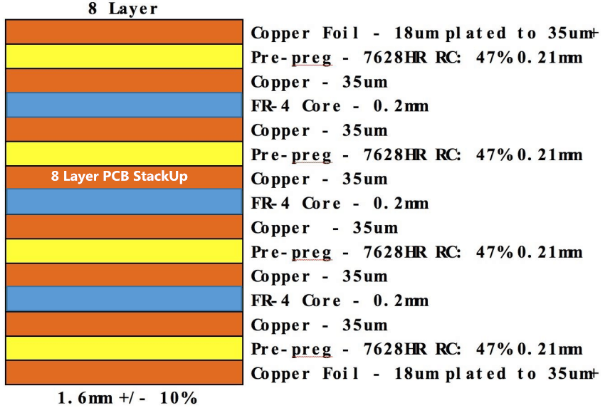
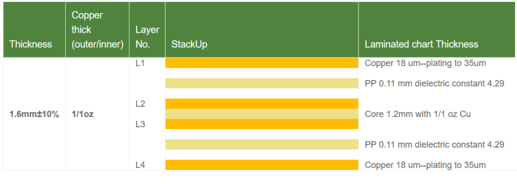
8 Layer PCB
Optimized for networking equipment, DDR memory routing, and telecom infrastructure systems.
- Multiple reference planes
- DDR3 / DDR4 compatible
- Better SI & EMI performance
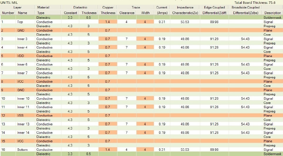
10 Layer PCB
Designed for demanding applications requiring controlled impedance and high-density routing capability.
- Controlled impedance design
- Advanced EMI suppression
- High-reliability stack-up
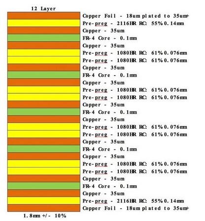
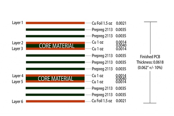
12 Layer PCB
Sequential lamination and HDI technology for servers, storage, and telecom backplanes.
- HDI structure support
- 25Gbps+ signal routing
- High routing density
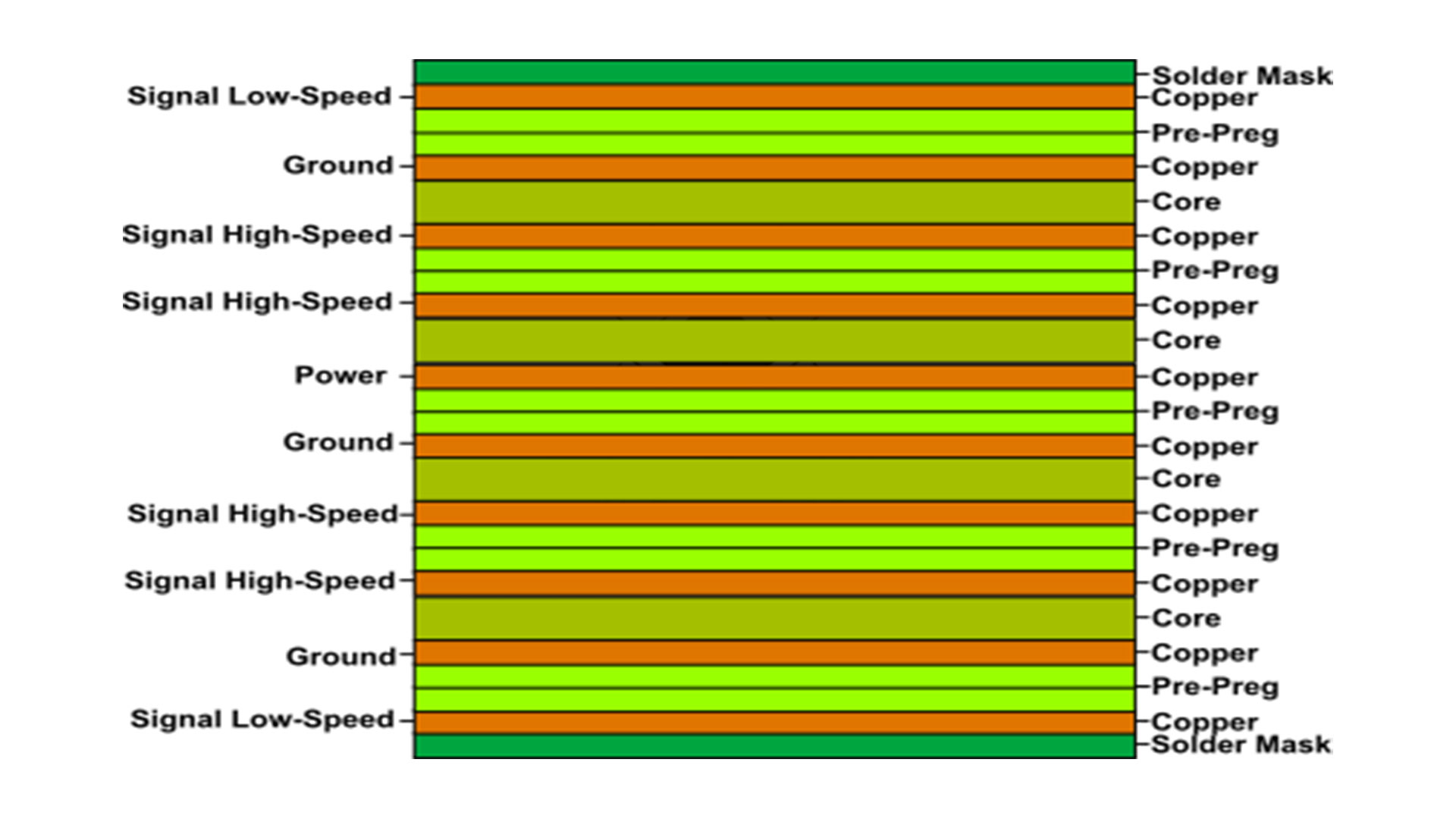
14 Layer PCB
Ultra-complex routing architecture supporting multiple voltage domains and high-speed backdrill structures.
- Backdrill compatible
- Via-in-pad technology
- Extreme signal integrity
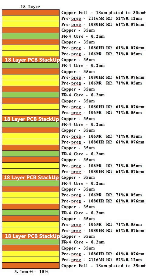
14+ Layers PCB
Custom high-layer-count PCB solutions for AI computing, military systems, data centers, and advanced networking.
- Up to 64-layer capability
- Sequential lamination
- Ultra-low-loss materials
Layer Cost & Lead Time Comparison
Understand how PCB layer count impacts fabrication complexity, manufacturing cost, and production lead time.
| Layer Count | Recommended Applications | Typical Stack-up | Relative Cost | Lead Time |
|---|---|---|---|---|
|
4 Layer
|
IoT, consumer electronics | Signal-GND-PWR-Signal | $ 1x baseline | 5-7 Days |
|
6 Layer
|
Industrial, automotive ECU | Sig-GND-Sig-Sig-PWR-Sig | $$ 1.3x | 6-8 Days |
|
8 Layer
|
Networking, telecom | Dual internal routing layers | $$$ 1.6x | 7-9 Days |
|
10 Layer
|
Medical & aerospace | Multiple reference planes | $$$$ 2.0x | 8-10 Days |
|
12 Layer
|
AI servers, high-speed systems | Sequential lamination + HDI | $$$$$ 2.4x | 9-12 Days |
|
14-24 Layer
|
Military, HPC, avionics | Advanced sequential stack-up | $$$$$$ 2.8x-4x | 10-14 Days |
24+ layer stack-ups are available with sequential lamination, backdrill, blind/buried vias, and advanced impedance control.
Contact Engineering →Material & Technical Parameters
Engineered material systems and precision fabrication capabilities for high-speed multilayer PCB manufacturing.
Optimized Stack-up Materials for High-Speed Applications
From standard FR-4 to ultra-low-loss laminates, Topfast provides stable dielectric performance, thermal reliability, and signal integrity support for advanced multilayer PCB designs.
Standard FR-4
GeneralStable and economical substrate solution for industrial electronics and consumer multilayer PCB designs.
High-Tg
AutomotiveEnhanced thermal stability and dimensional consistency for harsh environment electronics.
Rogers / Megtron
RF & AIUltra-low-loss laminates designed for RF, microwave, AI servers, and ultra-high-speed systems.
Need Help Selecting Materials?
Get stack-up suggestions and impedance optimization from our engineering team.
Request Consultation →How Many Layers Do You Need?
Optimize routing density, signal integrity, and manufacturing cost with the right multilayer PCB stack-up.
A Smarter Approach to Multilayer PCB Design
Selecting the correct layer count is one of the most critical decisions in PCB design. Too few layers can create routing congestion and EMI problems, while excessive layers increase cost and fabrication complexity.
Analyze Signal & Power Nets
Count high-speed interfaces, power domains, and differential pairs.
Estimate Routing Density
Evaluate available routing channels based on component density and board size.
Review High-Speed Requirements
Determine impedance control, EMI shielding, and return path requirements.
Optimize Stack-up with Engineers
Validate stack-up structure, material selection, and manufacturability.
72% of first-time multilayer PCB designs use more layers than necessary.
Our engineering team helps optimize stack-up structure to reduce fabrication cost while maintaining signal integrity and EMC performance.
Free Layer Analysis →Industry Certifications
International standards supporting stable multilayer PCB manufacturing, traceability, and long-term reliability.
Trusted Quality Standards for Critical Electronics
From automotive electronics to high-speed communication systems, Topfast follows globally recognized manufacturing and inspection standards to ensure every multilayer PCB meets strict performance and reliability requirements.

Quality Management System

Automotive Electronics Standard

Environmental Management

Product Safety Certification

IPC Electronics Acceptability
Success Stories
Proven multilayer PCB solutions delivered across medical, telecom, automotive, aerospace, and AI computing industries.
Ultrasound Imaging Module
Achieved 0.8mm BGA pitch routing with blind vias and optimized grounding strategy, reducing signal noise by over 40%.
100G Switch Backplane
Controlled impedance within ±5% and validated signal integrity performance for 28Gbps high-speed lanes.
AI Accelerator Platform
Sequential lamination with 0.1mm laser vias supporting high-density GPU architecture and stable mass production.
High-Reliability ECU
High-Tg material stack-up qualified for harsh automotive environments from -40°C to 150°C operation.
Avionics Control Module
Combined conformal coating, vibration testing, and via-in-pad structures for high-density avionics applications.
High-Speed Storage Controller
Backdrill technology optimized for 56G PAM4 signal integrity and ultra-low insertion loss performance.
Frequently Asked Questions
Ready to Start Your Multilayer PCB Project?
Upload your Gerber files, stack-up requirements, or BOM list. Our engineering team will review manufacturability, impedance, and layer optimization within 6 hours.