Table of Contents
Introduction
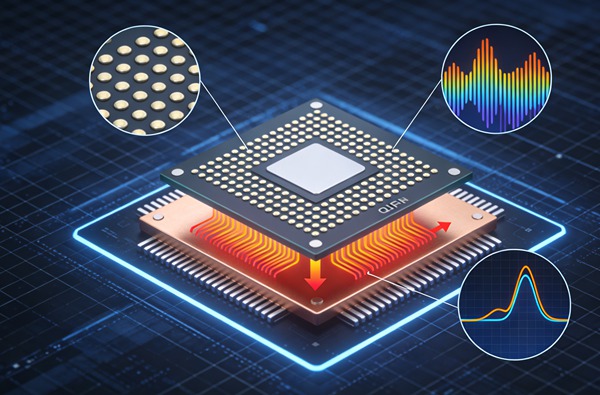
Quad Flat No-Lead (QFN) packages have become a ubiquitous choice in modern printed circuit board assembly (PCBA). Their compact form factor, exceptional electrical performance, and superior thermal dissipation capabilities make them ideal for everything from mobile devices to high-reliability aerospace and automotive applications. A defining feature of the QFN package is the large central exposed pad (thermal pad), which is designed to be soldered directly to the PCB to facilitate heat transfer and provide a robust electrical ground connection. Learn more about Heavy Copper PCBs: Thermal Management in Electric Vehicle (EV) Chargers.
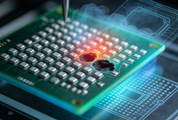
However, achieving a reliable, void-free solder joint under this large thermal pad is a persistent and complex challenge for PCB process and manufacturing engineers. Solder voiding—the formation of gas pockets or cavities within the solder joint—is arguably the most critical defect associated with QFN assembly. While a small, distributed amount of voiding is inevitable and generally acceptable, excessive voiding compromises the fundamental advantages of the package design.
High levels of solder voiding act as a thermal insulator, preventing efficient heat dissipation from the silicon die to the PCB, which can lead to thermal runaway and premature component failure. Furthermore, voids reduce the mechanical strength of the solder joint and can negatively impact the electrical impedance of high-frequency RF circuits. According to industry standards such as IPC-A-610, the maximum allowable voiding area is typically around 25% to 30%, though high-power or high-reliability applications often dictate much stricter internal limits, sometimes pushing for less than 10%. This article delves deep into the root causes of solder voiding under QFN components and explores how advanced thermal profiling and process engineering can effectively mitigate this pervasive issue.
Understanding the Root Causes of Solder Voiding in QFN Packages
To effectively eliminate or reduce solder voiding, it is crucial to first understand the mechanisms that drive its formation. Solder voids are fundamentally trapped gases, and identifying the source of these gases and why they fail to escape before the solder solidifies is the key to root cause analysis.
Flux Outgassing and Volatile Entrapment
The primary contributor to solder voiding is the outgassing of flux volatiles during the reflow process. Solder paste is a suspension of metal alloy powder in a flux medium. As the PCB passes through the reflow oven, the flux activates to remove oxides, and its volatile solvents begin to evaporate and outgas. Because the QFN thermal pad presents a large, continuous planar area with a very low standoff height, the escape path for these gaseous volatiles is highly restricted. If the solder reaches its liquidus state before the flux has fully outgassed, the remaining gases become permanently entrapped within the molten solder, forming voids upon cooling.
Stencil Aperture Design and Paste Volume
The design of the stencil used to print solder paste onto the PCB thermal pad is a critical variable. Printing a single, massive block of solder paste matching the exact dimensions of the thermal pad almost guarantees severe voiding. This approach traps flux volatiles in the center of the pad with no geometric channels for escape. Furthermore, an excessive volume of solder paste can cause the QFN package to “float” or tilt during reflow, leading to inconsistent standoff heights and exacerbating both voiding and the risk of bridging on the peripheral I/O pads. Learn more about Biocompatible PCBs: Advanced Materials for Implantable Medical Devices.
PCB Surface Finish and Pad Wettability
The metallurgical interaction between the solder paste, the PCB surface finish, and the component termination finish plays a significant role in void formation. If the PCB surface finish (such as OSP, ENIG, or Immersion Silver) is degraded due to poor storage, handling, or multiple thermal excursions, wettability is compromised. Similarly, if the QFN thermal pad itself is oxidized, the molten solder will not spread evenly and quickly. Poor wetting forces the flux to work harder and longer, generating more gas, while the uneven, sluggish spread of the solder creates localized pockets where gas is easily trapped. Learn more about Glass Substrates in PCB: The Future of High-Frequency IC Packaging.
Via-in-Pad Design Flaws
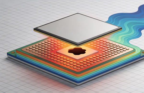
Many PCB designs utilize thermal vias directly beneath the QFN pad to transfer heat to internal ground planes or the opposite side of the board. If these vias are left un-tented or un-plugged, they act as capillary tubes. During reflow, molten solder wicks down into the vias, pulling air up into the joint and simultaneously starving the thermal pad of required solder volume. This interaction not only creates large macro-voids but also unpredictable variations in the thermal pad joint thickness.
The Crucial Role of Thermal Profiling
While stencil design and material selection are foundational, the thermal reflow profile is the dynamic control lever that dictates how those materials behave in real-time. An unoptimized reflow profile can induce severe voiding even with a perfect stencil design, whereas a finely tuned profile can often salvage a marginal design setup.
The standard reflow profile consists of four primary zones: pre-heat, soak, reflow (time above liquidus), and cooling. Each zone must be meticulously calibrated. If the pre-heat ramp rate is too aggressive, volatile solvents may boil violently, causing solder spatter and premature flux exhaustion. If the soak zone is too short or too cold, the flux will not fully activate, and oxides will remain, impeding wetting. Conversely, if the soak is too long or too hot, the flux may burn off entirely before the solder melts, eliminating its protective and wetting properties during the critical liquidus phase.
The Time Above Liquidus (TAL) and the peak temperature are the phases where voiding is finalized. The solder must remain fluid long enough for the surface tension to pull the component into place and for trapped gases to buoy to the edge of the joint and escape. However, excessive TAL can lead to intermetallic compound (IMC) embrittlement, while an insufficient peak temperature will result in sluggish, viscous solder that traps bubbles before they can migrate outward. Learn more about Burn-In Boards: High-Density Blind/Buried Vias for High-Pin Count Devices.
How to Optimize Thermal Profiling for QFN Void Reduction (Step-by-Step Guide)
Follow these engineering rules.
- Establish an Accurate Baseline Profile
Begin by attaching high-quality thermocouples directly to a fully populated test board. Crucially, at least one thermocouple must be placed directly under the QFN package by drilling through the back of the PCB into the thermal pad area. Relying solely on surface-level thermocouples is insufficient, as the thermal mass of the QFN will cause the actual joint temperature to lag significantly behind the surrounding board surface. Run this instrumented board through your standard profile to establish an accurate baseline of current conditions.
- Implement a Saddle or Extended Soak Profile
If your baseline profile is a traditional linear ramp-to-spike (RTS) profile, consider transitioning to a ramp-soak-spike (RSS) or “saddle” profile. Extend the soak zone time (typically between 150°C and 190°C for lead-free alloys) to allow maximum time for flux volatiles to outgas before the alloy transitions to a liquid state. The precise duration of the soak should be dictated by the solder paste manufacturer’s technical data sheet, but extending it toward the upper allowable limit often provides the necessary outgassing window for large thermal pads.
- Calibrate Time Above Liquidus (TAL) and Peak Temperature
Once outgassing is maximized during the soak, focus on the liquidus phase. Ensure the peak temperature is sufficient to reduce the viscosity of the molten solder, making it easier for trapped bubbles to move and escape. For SAC305 alloys, a peak temperature of 240°C to 245°C under the QFN is often optimal. The TAL must be long enough to allow these bubbles to clear the perimeter of the pad. Aim for a TAL of 60 to 90 seconds, carefully monitoring to ensure you do not exceed the thermal limits of other sensitive components on the board.
- Control the Cooling Rate
The cooling zone is often overlooked but is critical for final void mitigation. A rapid cooling rate solidifies the solder quickly, which can trap remaining bubbles in place, but it also creates a finer, stronger grain structure in the solder joint. Conversely, a very slow cooling rate allows more time for voids to escape but can lead to grainy, brittle joints. Aim for a controlled cooling rate of 2°C to 4°C per second. This balances the need for structural integrity with the final opportunity for gas expulsion.
- Validate with Automated X-Ray Inspection (AXI)
Thermal profiling is an iterative process. After adjusting the profile, run test boards and immediately subject them to 2D or 3D X-Ray inspection. Analyze the voiding percentage, void size distribution, and void location under the QFN. Use this empirical data to make micro-adjustments to the soak time, TAL, or peak temperature. Repeat this validation loop until the voiding consistently falls well below your internal quality thresholds.
Optimizing the thermal profile specifically for QFN packages requires a deliberate approach that balances flux chemistry requirements with the physical thermodynamics of a low-standoff component. Follow these steps to refine your profiling strategy.
Advanced Process Considerations Beyond Profiling
While thermal profiling is critical, it must work in concert with optimized design and material strategies to achieve the lowest possible voiding rates.
Stencil Aperture Optimization: Never use a 1:1 aperture for a QFN thermal pad. Instead, implement a “window pane” or grid array design. Break the large aperture into a matrix of smaller squares, separated by 0.2mm to 0.5mm web grids. This creates physical channels for flux outgassing. Target a paste coverage of 50% to 80% of the total pad area. As the solder melts, the separate deposits will flow together, pushing gas out through the grid channels.
Via Management Strategies: If thermal vias are necessary within the pad, they must be properly managed. The most reliable solution is to specify copper-plated, epoxy-filled, and planarized vias (IPC-4761 Type VII). If cost constraints prohibit this, vias should be tented with solder mask on the bottom side of the PCB to prevent solder wicking, though this still leaves a small cavity on the top side that can trap air.
Nitrogen Reflow Environment: Utilizing a nitrogen-inerted atmosphere in the reflow oven significantly widens the process window. Nitrogen displaces oxygen, drastically reducing the oxidation rate of the PCB pads, component terminations, and the molten solder powder itself. This improved wettability allows the solder to spread more rapidly and evenly, reducing the localized trapping of flux volatiles and lowering overall voiding percentages.
Vacuum Reflow Technology: For critical applications where voiding must be strictly kept below 5% or 10%, standard atmospheric profiling may not be enough. Vacuum reflow ovens apply a vacuum during the liquidus stage of the profile. This pressure differential actively pulls entrapped gas bubbles out of the molten solder before it is allowed to cool and solidify, offering the most definitive mechanical solution to voiding.
Solder Paste Selection: Evaluate the rheology and powder size of your solder paste. A paste with a more active flux chemistry or an anti-voiding formulation can help. Furthermore, switching from a Type 3 powder to a Type 4 or Type 5 powder can alter the outgassing dynamics and improve print release on complex stencil grids, indirectly contributing to void reduction.
Conclusion
Solder voiding under QFN packages is a multifaceted problem that cannot be solved by a single magic bullet. It requires a holistic, systematic approach that bridges PCB layout, stencil design, material selection, and rigorous thermal process engineering. By understanding the root causes of volatile entrapment and meticulously optimizing the reflow thermal profile—specifically through extended soak times, controlled peak temperatures, and calibrated time above liquidus—engineers can drastically reduce voiding levels. When combined with intelligent stencil aperture design, robust via management, and environmental controls like nitrogen, high-reliability, low-void QFN assembly is a highly achievable standard.
Frequently Asked Questions (FAQ)
Industry standards like IPC-A-610 generally accept up to 25% to 30% total voiding area in the thermal pad joint, provided there are no single massive voids bridging critical areas. However, for high-power, RF, or automotive applications, engineering requirements frequently demand less than 15% or even less than 10% voiding to ensure adequate thermal transfer and long-term reliability.
Practically speaking, zero percent voiding is nearly impossible to achieve in a standard atmospheric SMT reflow process due to the fundamental nature of flux chemistry outgassing. The goal is not complete elimination, but rather the systematic reduction and control of voids to levels that do not impact the electrical, thermal, or mechanical performance of the product. Specialized vacuum reflow ovens can reduce voiding to near zero (often <1%), but these represent a significant capital investment.
Stencil thickness dictates the total volume of solder paste deposited. A thicker stencil (e.g., 5 to 6 mils) deposits more volume, which can lead to component float, increased bridging risks on the peripheral pads, and higher voiding due to a larger volume of flux that needs to outgas. Often, stepping down the stencil thickness specifically over the thermal pad area, or utilizing a thinner global stencil (e.g., 4 mils) with a highly optimized window-pane aperture, yields significantly better results.
While not strictly mandatory for all commercial assemblies, nitrogen reflow is highly recommended for complex QFN and BGA processing. The inert atmosphere dramatically improves wetting by preventing oxidation during the heating cycle. This faster, more uniform wetting prevents the solder from rolling over and trapping gas pockets, making it one of the most effective operational tools for reducing voiding without altering the physical design of the board.
A linear (Ramp-to-Spike) profile increases temperature at a steady, continuous rate until peak reflow. This can sometimes cause the flux to activate and the solder to melt simultaneously, trapping rapidly expanding volatiles within the joint. A soak (Ramp-Soak-Spike) profile includes a specific plateau zone where the temperature is held steady (or rises very slowly) just below the melting point of the alloy. This provides the flux ample time to fully outgas its solvents before the solder turns liquid, significantly reducing the volume of gases available to form voids during the liquidus phase.