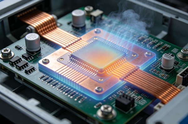
As the global transition towards sustainable transportation accelerates, the demand for electric vehicles (EVs) has surged dramatically. This shift necessitates a robust and pervasive infrastructure, specifically high-power EV chargers capable of delivering rapid, reliable charging to alleviate driver range anxiety. Level 3 DC fast chargers, for instance, can deliver anywhere from 50 kW to 350 kW and beyond, imposing immense electrical and thermal stresses on their internal electronic components. At the heart of these high-power systems lie Printed Circuit Boards (PCBs) that must endure extreme currents and elevated temperatures without failure. To meet these rigorous and demanding specifications, engineers increasingly turn to heavy copper PCBs.
This comprehensive guide explores the critical role of heavy copper PCBs in managing the thermal and electrical challenges inherent in EV charger design, providing actionable insights for engineering robust power electronics. Learn more about AXI X-Ray Inspection: Detecting PTH Fill and Barrel Cracking Defects.
Table of Contents
The Imperative for Advanced Thermal Management in EV Chargers
Electric vehicle chargers operate by converting AC power from the grid into DC power suitable for the vehicle’s battery, or by directly routing high-voltage DC power. This intricate process involves complex power electronics, including rectifiers, inverters, DC-DC converters, and specialized switching components like Insulated-Gate Bipolar Transistors (IGBTs) and Silicon Carbide (SiC) MOSFETs. When hundreds of amperes of current flow through these components and the PCB traces connecting them, significant heat is generated due to resistive losses, a phenomenon known as Joule heating. Learn more about Automotive PCB Reliability: Understanding IPC-6012 Class 3 vs Class 3A.
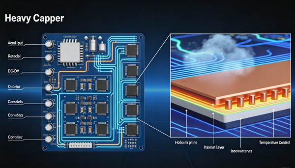
If not properly managed, this localized heating can lead to a cascade of detrimental effects. Elevated temperatures accelerate the degradation of semiconductor components, reduce the lifespan of dielectric materials, and can induce severe mechanical stress due to differing Coefficients of Thermal Expansion (CTE) within the PCB assembly. This stress often manifests as delamination, fractured vias, or broken solder joints, ultimately resulting in catastrophic system failure. Effective thermal management is not merely a performance enhancement; it is a fundamental requirement for the safety, longevity, and operational reliability of EV charging infrastructure.
Understanding Heavy Copper PCBs
In standard PCB manufacturing, copper weights typically range from 0.5 oz/ft² (approximately 17.5 µm thick) to 2 oz/ft² (approximately 70 µm thick). A heavy copper PCB, conversely, is generally defined as a board utilizing copper weights ranging from 3 oz/ft² (105 µm) up to 20 oz/ft² (700 µm) or more on its inner or outer layers. Extreme copper variants can push these limits even further for highly specialized industrial applications.
The fundamental advantage of heavy copper lies in its significantly increased cross-sectional area. By growing the trace thickness vertically, layout designers can achieve massive current-carrying capacities without requiring impractically wide traces that would consume valuable board real estate. This vertical expansion is crucial in modern EV chargers, where miniaturization and high power density are constant and critical design objectives.
Key Benefits for High-Power Applications
The integration of heavy copper into PCB designs offers several distinct advantages that are uniquely suited to the specific challenges of EV charger development. Learn more about Medical PCB Assembly: ISO 13485 Compliance & Traceability.
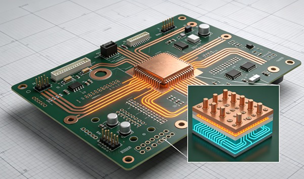
Enhanced Current Carrying Capacity: The most immediate and obvious benefit is the ability to conduct very high currents with minimal resistive voltage drop (I²R losses). This ensures highly efficient power delivery from the grid interface directly to the vehicle connector.
Superior Heat Dissipation: Copper is an excellent thermal conductor. Thick copper planes act as built-in heat spreaders, effectively wicking thermal energy away from localized hot spots generated by power components and distributing it evenly across the entire board surface area. This significantly lowers the junction temperatures of critical semiconductors.
Increased Mechanical Strength: Heavy copper significantly reinforces the mechanical integrity of the PCB itself and the plated through-hole (PTH) vias connecting different layers. This added robustness is vital for EV chargers that may be subjected to physical shock, vibration, and extreme thermal cycling in harsh outdoor environments.
Reduction of Bulky Wiring: By routing high currents directly through the PCB, designers can eliminate or heavily reduce the need for bulky, expensive, and difficult-to-assemble external busbars or cumbersome wire harnesses, streamlining the manufacturing process and improving overall system reliability.
Design Considerations for Heavy Copper PCBs
Designing with heavy copper requires a distinct paradigm shift from standard digital or low-power analog layout techniques. Engineers must meticulously balance electrical performance, thermal dissipation, and complex manufacturability constraints.
Trace Width and Spacing (Creepage and Clearance)
High-power EV chargers operate at dangerous voltage levels, often exceeding 800V DC in modern architectures. Consequently, strict adherence to creepage (the shortest path between two conductive parts along the surface of the insulation) and clearance (the shortest distance through air) standards is mandatory to prevent electrical arcing and dielectric breakdown. When designing with heavy copper, the manufacturing process—specifically the etching of thick metal—results in a trapezoidal trace cross-section due to undercutting. This “etch factor” must be accounted for in the layout, requiring larger minimum spacing between traces than what would be acceptable on standard boards to guarantee the required electrical isolation.
Thermal Vias and Heat Sinks
While heavy copper successfully spreads heat laterally across the board, moving heat vertically through the FR-4 substrate to external cooling mechanisms requires thermal vias. These are plated through-holes strategically placed directly under high-power components to create a low-thermal-resistance path to underlying copper planes or to an external heat sink. In some extreme designs, solid copper coins are embedded directly into the PCB substrate beneath critical components to provide an unparalleled thermal pathway. Learn more about Flex PCB Stiffeners: Choosing Between FR4, Polyimide, and Stainless Steel.
Substrate Material Selection
The extreme heat generated within EV chargers demands substrate materials that can withstand prolonged high-temperature exposure without degrading. Standard FR-4 may break down over time under these harsh conditions. Engineers should specify high-Tg (Glass Transition Temperature) materials (Tg > 170°C) and materials with a very low CTE in the Z-axis to prevent via barrel cracking during continuous thermal expansion and contraction. Materials like polyimide or specialized thermally conductive dielectrics are often strictly necessary for heavy copper applications in these demanding environments.
How to Design a Heavy Copper PCB for EV Chargers (Step-by-Step Guide)
Follow these engineering rules.
- Define Power Requirements and Current Profiles
Begin by establishing the absolute maximum and continuous operating currents for every high-power net in the entire system. Identify the peak transient currents that occur during turn-on sequences or fault conditions. Simultaneously, determine the maximum allowable temperature rise for the PCB traces and the absolute maximum junction temperatures for all power semiconductors based on the ambient operating environment of the charger.
- Select the Appropriate Copper Weight
Utilize industry standards such as IPC-2221 (Generic Standard on Printed Board Design) or IPC-2152 (Standard for Determining Current Carrying Capacity in Printed Board Design) to calculate the minimum required cross-sectional area for your high-current traces. Based on your specific board size constraints, select a copper weight (e.g., 4 oz, 6 oz, 10 oz) that allows you to achieve this required cross-sectional area with reasonable and routable trace widths.
- Plan the Layer Stackup
Develop a specialized layer stackup that strategically positions heavy copper layers for maximum effect. Often, outer layers utilize extremely heavy copper for connecting large power terminals and dissipating heat to ambient air, while inner layers might use moderately heavy copper for bulk power distribution routing. Ensure sufficient dielectric thickness between high-voltage layers to strictly meet all safety isolation requirements.
- Route High-Current Traces
Route the high-power paths first before any sensitive control signals. Keep these traces as short and direct as possible to minimize parasitic inductance and resistance. Avoid 90-degree angles or sharp corners entirely; instead, use 45-degree angles or gentle curves to prevent current crowding and the subsequent formation of localized hot spots. Ensure solid, continuous ground returns underneath high-frequency switching nodes to minimize electromagnetic interference (EMI).
- Implement Thermal Vias and Heat Sinks
Place dense arrays of thermal vias directly beneath heat-generating components like power field-effect transistors (FETs) and high-current diodes. Ensure these vias connect solidly and broadly to the internal heavy copper planes. If the board interfaces with a mechanical heat sink, design the component placement and thermal via structures to align optimally with the heat sink’s contact area, and carefully specify appropriate Thermal Interface Materials (TIMs).
- Perform Thermal Simulation
Before finalizing the layout for prototyping, employ computational fluid dynamics (CFD) or finite element analysis (FEA) thermal simulation software. Import your finalized PCB layout and component power dissipation profiles to digitally model the temperature distribution across the board. This step is absolutely critical for identifying potential hidden thermal bottlenecks and verifying that your copper weights, trace widths, and via structures are sufficient to keep temperatures well within safe operating limits.
- Finalize Design Rules for Manufacturability
Collaborate closely with your chosen PCB fabrication partner early in the design cycle. Heavy copper etching and lamination are highly specialized processes with unique constraints. Ensure your design meticulously adheres to their specific Design for Manufacturability (DFM) guidelines regarding minimum trace width, minimum spacing, via aspect ratios, and the application of solder mask over exceptionally thick traces. Adjust your layout as necessary to guarantee high manufacturing yields and long-term board reliability. Manufacturing Challenges and Considerations Producing heavy copper PCBs is significantly more complex and resource-intensive than standard board fabrication. The primary challenge lies in the copper etching process. Etching through a thick layer of copper takes considerably longer, and the chemical etchant solution attacks the sides of the trace (undercutting) as it eats downwards. This results in a trace that is physically narrower at the top than at the base. PCB fabricators must employ highly specialized etching techniques and precise timing to manage this, and designers must provide adequate spacing tolerances in their CAD tools. Furthermore, laminating multi-layer heavy copper boards requires careful control of resin flow dynamics. The deep physical valleys between thick copper traces must be completely filled with prepreg resin during the high-pressure pressing process to prevent air voids. These voids could severely compromise the dielectric strength of the board and lead to high-voltage arcing. Fabricators often use higher resin content prepregs and heavily modified lamination thermal profiles to ensure a solid, reliable, void-free board structure. Finally, the immense thermal mass of heavy copper boards makes them notoriously difficult to solder using standard surface mount technology (SMT) reflow profiles. Solder reflow ovens must be carefully custom-profiled to ensure the entire board reaches the solder liquidus temperature without thermally damaging heat-sensitive components. Hand soldering heavy copper boards is nearly impossible without specialized high-power soldering irons or aggressive thermal pre-heaters. Conclusion The widespread proliferation of electric vehicles inherently hinges on the availability of fast, dependable, and ubiquitous charging networks. Heavy copper PCBs act as the unsung heroes of this vital infrastructure, providing the critical foundational backbone necessary to manage the immense power and thermal loads involved in rapid EV charging. By thoroughly understanding the unique thermal dynamics at play, rigidly adhering to specialized high-power design principles, and collaborating closely with experienced fabrication partners, engineers can successfully leverage heavy copper technology. Doing so enables the creation of EV chargers that are not only extraordinarily powerful and efficient but also exceptionally safe and reliable for years of continuous operation in the most demanding real-world environments.
Designing a heavy copper board for an EV charger is a highly iterative process that demands careful upfront planning and rigorous validation.
Frequently Asked Questions (FAQ)
Generally, any printed circuit board that utilizes copper weights exceeding 3 ounces per square foot (oz/ft²) on either its inner or outer layers is classified by the industry as a heavy copper PCB. In highly demanding power electronics applications, such as commercial EV chargers, these copper weights can routinely scale up to 10 oz/ft², 20 oz/ft², or even higher to accommodate massive current flows.
While wider traces can theoretically carry more electrical current, EV chargers often face strict spatial and form-factor limitations to keep the overall enclosure size manageable and cost-effective. Heavy copper allows engineering teams to achieve the necessary high current-carrying capacity within a highly compact PCB footprint by expanding the trace cross-sectional area vertically rather than horizontally across the board surface.
Not necessarily. While heavy copper acts as a highly effective internal heat spreader—rapidly moving thermal energy away from localized hot spots and distributing it across the broader board area—the sheer volume of heat generated by ultra-high-power components (like SiC MOSFETs operating in a 350kW fast charger) typically still necessitates the use of external metal heat sinks, forced air cooling fans, or even sophisticated liquid cooling systems to expel the accumulated heat into the ambient environment safely.
Yes, the heavy copper manufacturing process requires specific layout tolerances. Etching thick copper chemically inevitably results in “undercutting,” creating a trapezoidal trace profile that is significantly wider at the base than at the top surface. Designers must factor in this specific “etch factor” by proactively increasing the minimum spacing between adjacent traces. This ensures they meet the stringent electrical clearance rules required for high-voltage applications and actively prevent potential short circuits during operation.
In the vast majority of high-power cases, standard FR-4 is insufficient. The consistently high operating temperatures and extreme thermal cycling typical of high-power EV chargers require advanced, ruggedized substrate materials. Engineers typically specify high-Tg (Glass Transition Temperature) FR-4 variants, robust polyimide, or specialized thermally conductive dielectrics. These premium materials offer excellent thermal stability, high dielectric strength, and a tightly controlled Coefficient of Thermal Expansion (CTE) to actively prevent mechanical failures like layer delamination or cracked vias over the product’s lifespan.