Table of Contents
Introduction to Automotive PCB Reliability
The automotive industry is undergoing an unprecedented transformation. With the rapid proliferation of Advanced Driver Assistance Systems (ADAS), the transition to complex Electric Vehicle (EV) powertrains, and the relentless march toward fully autonomous driving, the electronic content within a modern vehicle has surged exponentially. In this landscape, the printed circuit board (PCB) is no longer a simple substrate for connecting components; it is the central nervous system of a multi-ton machine operating in highly unpredictable and harsh environments.
Automotive electronics face environmental stressors that rival, and sometimes exceed, those found in aerospace applications. These include extreme thermal cycling (ranging from -40°C in arctic conditions to over +150°C in under-hood compartments), severe and sustained multi-axis vibration, high humidity, and exposure to corrosive chemicals. In safety-critical systems such as brake-by-wire, steering-by-wire, and autonomous decision-making modules, a single point of failure can lead to catastrophic outcomes. Learn more about Dynamic Flex PCBs: Enhancing Bending Cycles in Wearable Devices.
Consequently, ensuring the absolute reliability of these electronic assemblies is paramount. To achieve this, automotive engineers and PCB designers rely on rigorous manufacturing and performance standards, primarily those defined by the IPC (Association Connecting Electronics Industries). Among these, the IPC-6012 standard—”Qualification and Performance Specification for Rigid Printed Boards”—serves as the definitive benchmark. For mission-critical applications, the debate often centers on the stringent requirements of IPC-6012 Class 3 versus the ultra-exacting criteria of Class 3A. Understanding the nuanced engineering differences between these two tiers is crucial for designing automotive PCBs that deliver flawless performance over a vehicle’s lifespan.
Understanding the IPC-6012 Standard and Performance Classes
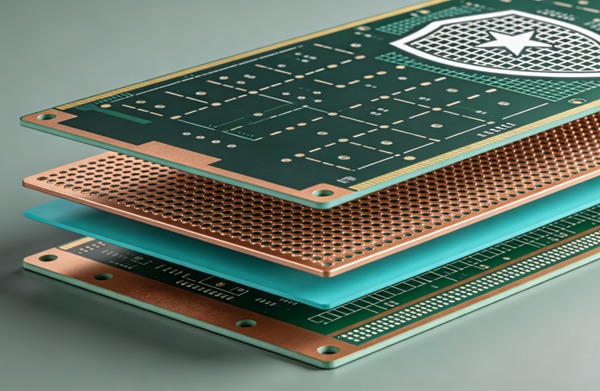
The IPC-6012 standard establishes comprehensive requirements for the fabrication of rigid PCBs. It categorizes electronic products into three distinct performance classes based on their application, desired reliability, and the consequences of failure: Learn more about Glass Substrates in PCB: The Future of High-Frequency IC Packaging.
- Class 1 (General Electronic Products): Products where the primary requirement is the function of the completed assembly, typical of disposable consumer electronics.
- Class 2 (Dedicated Service Electronic Products): Products where continued performance and extended life are required, and for which uninterrupted service is desired but not critical. Standard automotive infotainment systems historically fell into this category.
- Class 3 (High-Reliability Electronic Products): Products where continued high performance or performance-on-demand is critical, equipment downtime cannot be tolerated, the end-use environment may be uncommonly harsh, and the equipment must function when required. This includes life-support systems, military equipment, and critical automotive safety systems.
For modern automotive engineering, especially concerning systems that dictate vehicle control and passenger safety, Class 3 is considered the baseline requirement. However, as automotive electronics have become more sophisticated and operating conditions more extreme, the standard Class 3 specifications are sometimes deemed insufficient for the highest tiers of reliability.
The Emergence of Class 3A and the IPC-6012DA Automotive Addendum
To address the unique demands of ultra-high reliability applications, IPC introduced “Class 3A” requirements, initially documented in addendums like IPC-6012DS (Space and Military Avionics). Class 3A represents a significant escalation in manufacturing precision, inspection stringency, and defect intolerance compared to standard Class 3.
Recognizing that the automotive sector was beginning to face reliability challenges akin to those in aerospace, the IPC developed the IPC-6012DA—the Automotive Applications Addendum to IPC-6012. This addendum bridges the gap between standard high-reliability manufacturing and the specific, grueling mission profiles of modern vehicles. While IPC-6012DA relies heavily on Class 3 baseline requirements, engineers designing for the most critical automotive systems (like Level 4 and Level 5 autonomous computing cores or 800V EV traction inverters) often mandate Class 3A level constraints for specific critical parameters to virtually eliminate the possibility of latent defects such as Conductive Anodic Filament (CAF) growth or Plated Through-Hole (PTH) fatigue.
Key Engineering Differences: IPC-6012 Class 3 vs. Class 3A
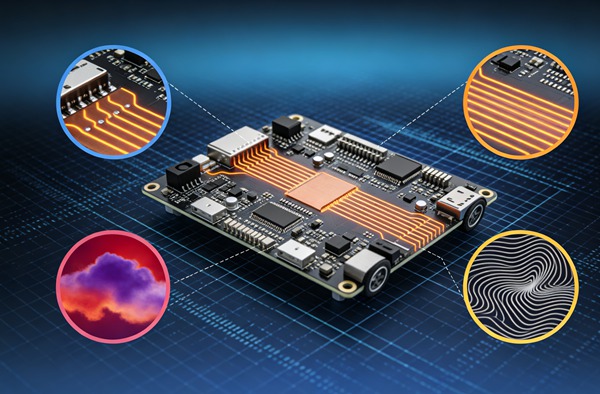
While both classes demand exceptional manufacturing quality, Class 3A leaves no room for manufacturing anomalies that might theoretically pass in a Class 3 board but could precipitate failure under severe thermomechanical stress. The critical technical differentiators include: Learn more about Cavity PCBs: Designing Recessed Cavities for RF Power Amplifiers.
Plated Through-Hole (PTH) Copper Thickness
The integrity of the copper plating in through-holes and microvias is the primary defense against interconnect failure during thermal cycling.
* Class 3: Requires a robust minimum average copper plating thickness in the PTH, typically specified at 25.4 µm (1.0 mil), with slight allowances for isolated thin areas provided they meet a defined absolute minimum.
* Class 3A: Mandates stricter controls on copper thickness. It generally requires a higher absolute minimum thickness (often >30 µm) and explicitly forbids any negative tolerance or localized thinning (voids) in the hole wall. The objective is to maximize the copper’s tensile strength and elongation capabilities to withstand the mechanical strain of Z-axis expansion of the FR4 dielectric material during extreme temperature excursions.
Annular Ring and Breakout Allowances
The annular ring is the area of copper pad remaining around a drilled hole. A robust annular ring ensures a solid electrical and mechanical connection between the via plating and the internal or external copper layers.
* Class 3: Demands a minimum external annular ring of 25.4 µm (1.0 mil) and generally prohibits hole breakout (where the drilled hole extends beyond the copper pad). However, some minor tangency might be acceptable under highly specific internal layer conditions if structural integrity is maintained.
* Class 3A: Enforces a zero-tolerance policy for any form of breakout or tangency. It often requires a larger minimum annular ring (e.g., 50 µm / 2.0 mils) to provide an overwhelming margin of safety against drill wander, layer misregistration, and thermal-mechanical fatigue. This significantly impacts Design for Manufacturability (DFM), requiring larger pad sizes which can conflict with High-Density Interconnect (HDI) routing requirements. Learn more about SMT Stencil Design: Nano-Coating and Step-Stencils for Mixed Technology.
Plating Voids
Plating voids are areas within the PTH where copper fails to deposit, exposing the underlying dielectric.
* Class 3: Permits a very limited number of small plating voids (typically no more than one per hole, not exceeding 5% of the total hole length, and occurring in a very small percentage of the total holes).
* Class 3A: Strictly prohibits any plating voids in the PTH. The presence of a void acts as a significant stress concentrator. Under the aggressive thermal cycling of an automotive engine compartment, a microscopic void can quickly propagate into a full circumferential crack, resulting in an open circuit.
Dielectric Spacing and Wicking
Wicking refers to the capillary action where copper plating solution penetrates the glass bundles of the laminate surrounding a drilled hole. Excessive wicking reduces the effective dielectric spacing between adjacent holes or copper features, increasing the risk of CAF failure—a critical concern in high-voltage EV architectures.
* Class 3: Limits copper wicking, typically allowing a maximum penetration of 80 µm (3.15 mils).
* Class 3A: Restricts wicking even further, often limiting it to 50 µm (1.97 mils) or less. Meeting this requirement necessitates optimized drilling parameters (feed and speed rates) to prevent fracturing the glass fibers, as well as the selection of high-quality, closely woven glass laminates and specialized desmear processes.
Etchback Requirements
Etchback is a chemical process used in multilayer boards to remove a small amount of the dielectric material from the hole wall prior to plating, exposing the internal copper layers on three sides. This creates a superior mechanical and electrical “three-point” connection.
* Class 3: May require positive etchback for maximum reliability, though flush connections can sometimes be acceptable depending on the specific application profile.
* Class 3A: Mandates tightly controlled positive etchback. The specification dictates precise minimum and maximum etchback depths (e.g., 0.2 mils to 0.8 mils). Too little etchback provides insufficient mechanical anchoring; too much can create structural weakness and pooling of plating solutions.
How to Implement IPC-6012 Class 3A in Automotive PCB Design (Step-by-Step Guide)
Follow these engineering rules.
- Define the Automotive Mission Profile
Before laying out a single trace, engineers must rigorously define the component’s operational lifecycle. This includes mapping the expected temperature extremes, thermal cycle frequency, vibration spectrum (random and sine), humidity levels, and required operational lifespan (e.g., 15 years / 300,000 miles). This mission profile dictates whether the extreme measures of Class 3A are truly required.
- Select High-Reliability Base Materials
Standard FR-4 is insufficient for Class 3A automotive applications. Engineers must specify advanced laminates with high Glass Transition Temperatures (Tg > 170°C), high Decomposition Temperatures (Td > 340°C), and low Coefficient of Thermal Expansion (CTE) in the Z-axis. Furthermore, materials must be CAF-resistant, utilizing specific resin formulations and tightly woven glass styles (like 1078 or 1080) to prevent the migration of conductive filaments under high-voltage bias.
- Design for Manufacturability (DFM) with Class 3A Constraints
Designing for Class 3A means relaxing certain high-density constraints to accommodate manufacturing tolerances that guarantee zero defects. This involves specifying larger via pads to ensure robust annular rings, increasing trace spacing to mitigate CAF risks, and minimizing the use of highly complex HDI structures (like deeply stacked microvias) which are statistically more prone to thermo-mechanical failure than staggered via configurations.
- Specify Exact Plating and Surface Finish Requirements
The fabrication drawing must explicitly call out Class 3A requirements. Do not rely on generic IPC-6012 callouts. Specify the exact minimum copper plating thickness required in the hole walls, mandate positive etchback dimensions, and enforce a zero-tolerance policy for plating voids and hole breakout. Select surface finishes that withstand multiple reflow cycles and automotive environments, such as ENIG (Electroless Nickel Immersion Gold) or ENEPIG.
- Implement Comprehensive Quality Assurance Protocols
Class 3A manufacturing requires extreme verification. Mandate advanced inspection techniques from your PCB fabricator. This includes requiring microsection (cross-section) analysis on every production panel to verify plating thickness, etchback, and wicking limits. Implement rigorous Automated Optical Inspection (AOI) and 100% electrical testing (flying probe or bed-of-nails) using high-voltage parameters to detect latent shorts or high-resistance interconnects.
Transitioning a design from standard commercial requirements to ultra-high reliability Class 3A standards requires a paradigm shift in both engineering approach and supply chain management.
The Manufacturing Reality: Cost vs. Reliability
Specifying IPC-6012 Class 3A comes with a significant economic impact. The rigorous controls required to achieve zero-defect manufacturing—including slower drilling speeds to prevent glass fiber damage, longer plating cycles to ensure adequate copper deposition, extensive microsection analysis, and higher scrap rates due to unforgiving tolerances—can increase bare board costs by 30% to 50% or more compared to standard Class 3.
Furthermore, very few PCB manufacturers possess the engineering expertise, specialized equipment, and stringent process controls necessary to consistently yield Class 3A product. The supply chain is constrained to elite fabricators primarily accustomed to servicing the aerospace and defense sectors.
However, in the context of an automotive recall, this initial investment is negligible. A single field failure in an autonomous braking system due to a microscopic PTH fatigue crack can result in devastating safety consequences, massive recall costs, and irreparable brand damage. For Tier 1 automotive suppliers and OEMs, the cost premium of Class 3A is not an expense; it is a vital insurance policy against catastrophic liability.
Conclusion
As the automotive industry continues its relentless drive toward electrification and autonomy, the definition of “reliable” must be continually recalibrated. While IPC-6012 Class 3 remains a highly robust standard suitable for many vehicle systems, the emergence of mission-critical, life-safety electronics necessitates the uncompromising stringency of Class 3A principles. By deeply understanding the technical nuances—from annular ring tolerances to wicking limits—and rigorously applying the IPC-6012DA addendum, automotive engineers can design PCBs that not only survive the brutal realities of the road but perform flawlessly when lives depend on them.
Frequently Asked Questions (FAQ)
While technically possible to specify different classes for different features on a fabrication drawing (a practice known as a “mixed class” board), it is highly discouraged in automotive applications. Manufacturing a board requires uniform physical and chemical processes. Attempting to apply relaxed Class 2 standards to certain areas while demanding Class 3 reliability elsewhere introduces process variations and inspection complexities that drastically increase the risk of overall board failure. A board should be manufactured to the highest class required by its most critical component.
No. IPC-6012DA (the Automotive Applications Addendum) provides specific modifications and enhancements to the base IPC-6012 standard tailored for automotive environments. It builds upon standard Class 2 and Class 3 requirements. However, it introduces concepts and testing protocols that align closely with Class 3A stringency, particularly regarding reliability testing (like thermal shock resistance). The decision to fully invoke the zero-defect tolerances of Class 3A remains an engineering decision based on the specific mission profile of the system.
The shift from 400V to 800V architectures in electric vehicles exponentially increases the risk of Conductive Anodic Filament (CAF) failure and dielectric breakdown. Higher voltages generate stronger electric fields that accelerate the electromigration of copper along the glass fiber interfaces within the PCB substrate. Consequently, the ultra-strict wicking limits, enhanced dielectric spacing requirements, and superior base material specifications mandated by Class 3A become critical necessities rather than optional upgrades for 800V powertrain electronics.
The cost premium varies significantly based on board complexity, layer count, and material selection. However, as a general rule of thumb, specifying strict Class 3A requirements can increase the bare PCB manufacturing cost by 30% to over 60% compared to a standard Class 3 board. This increase is driven by slower, more precise drilling feeds/speeds, longer plating cycles, significantly lower manufacturing yields (due to zero-tolerance inspection criteria), and the extensive destructive testing (microsectioning) required for compliance verification.