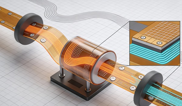
Table of Contents
Introduction to Dynamic Flex PCBs in Wearable Devices
The proliferation of wearable technology has dramatically shifted the paradigm of electronic design. Unlike traditional rigid electronics, wearable devices demand continuous, multi-axis movement while maintaining unwavering electrical reliability. At the core of this electromechanical challenge lies the Flexible Printed Circuit Board (Flex PCB), specifically designed for dynamic applications. Dynamic Flex PCBs are engineered not just to bend once for installation, but to endure thousands, or even millions, of bending cycles over their operational lifespan.
Understanding the mechanics of dynamic flex PCBs and mastering the design techniques to enhance their bending cycles is critical for engineers developing next-generation wearables, from medical monitoring patches and smart clothing to augmented reality headsets and fitness trackers. This article delves into the technical intricacies of dynamic flex PCBs, focusing on the material selections, stackup configurations, and routing methodologies necessary to maximize longevity and mechanical robustness.
The Mechanics of Bending in Flexible Circuits
To optimize a flex PCB for dynamic applications, it is essential to understand what happens at a microscopic level during a bending event. When a flex circuit is bent, the layers experience different mechanical stresses depending on their position relative to the neutral bend axis.
The Neutral Bend Axis
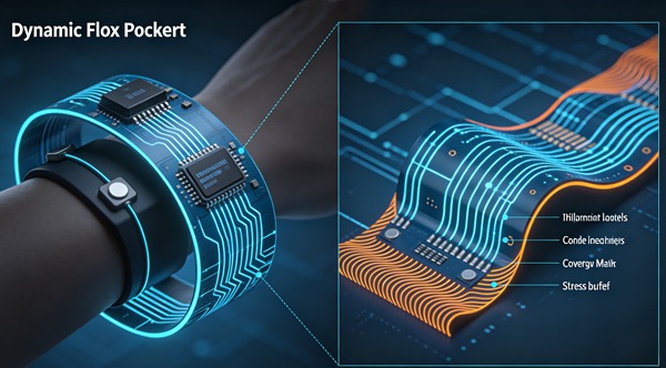
The neutral bend axis is the theoretical plane within the cross-section of the flex circuit where the material is under zero stress during a bend. Materials located on the outside of the bend radius are subjected to tensile stress (stretching), while materials on the inside are subjected to compressive stress (squeezing).
For a dynamic flex PCB, the primary design objective is to position the critical components—specifically the fragile copper traces—as close to the neutral bend axis as possible. By doing so, the tension and compression forces exerted on the copper are minimized, thereby drastically reducing the risk of work hardening, micro-cracking, and eventual trace fracture.
Strain and Bend Radius
The amount of strain placed on the copper traces is directly proportional to the thickness of the circuit and inversely proportional to the bend radius. The relationship is often approximated by the formula: Learn more about Metal Core PCBs (MCPCB): Aluminum vs. Copper Base for High-Power LEDs.
Strain (%) = (Thickness of Flex Circuit / (2 * Bend Radius)) * 100
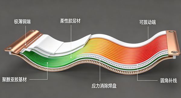
In dynamic applications, keeping the strain below 0.3% is generally recommended for maximizing bending cycles. This necessitates ultra-thin dielectric materials and carefully controlled bend radii. IPC-2223 standards provide excellent guidelines for minimum bend radii based on the type of flex circuit (e.g., single-sided, double-sided, multilayer) and the intended application (static vs. dynamic). Learn more about PTFE (Teflon) PCBs: Manufacturing and Plating Challenges for High-Frequency Boards.
Material Selection for Dynamic Flex PCBs
The foundation of a robust dynamic flex PCB lies in the selection of materials. Standard rigid PCB materials like FR4 are entirely unsuitable. Instead, engineers must specify advanced polyimides and specialized copper foils.
Polyimide (PI) Substrates
Polyimide is the industry standard for flexible dielectrics due to its exceptional thermal stability, chemical resistance, and mechanical flexibility. For dynamic applications, adhesiveless polyimide laminates are highly preferred.
Traditional laminates use an acrylic or epoxy adhesive to bond the copper foil to the polyimide core. These adhesives are thicker and less flexible than the polyimide itself, increasing the overall thickness of the circuit and shifting the neutral axis unpredictably. Adhesiveless laminates, on the other hand, cast the polyimide directly onto the copper (or vice versa), resulting in a significantly thinner, more reliable, and highly flexible substrate perfectly suited for millions of flexing cycles.
Copper Foil: Rolled Annealed (RA) vs. Electrodeposited (ED)
The type of copper foil used is arguably the most critical material decision for a dynamic flex circuit. There are two primary types: Electrodeposited (ED) and Rolled Annealed (RA).
- Electrodeposited (ED) Copper: Manufactured by electroplating copper onto a rotating drum. This process creates a columnar grain structure perpendicular to the surface. While excellent for high-density routing and rigid PCBs, ED copper is susceptible to cracking when subjected to repeated bending.
- Rolled Annealed (RA) Copper: Manufactured by repeatedly passing a copper ingot through heavy rollers, which elongates the grain structure horizontally, parallel to the surface. The copper is then annealed (heated and cooled) to relieve internal stresses. The elongated grain structure of RA copper acts like overlapping shingles, allowing it to flex and slide over itself significantly better than ED copper.
For wearable devices requiring high dynamic bending cycles, Rolled Annealed (RA) copper is universally mandated.
Coverlays and Solder Masks
To protect the copper traces on the outer layers, a coverlay is typically used instead of traditional liquid photoimageable (LPI) solder mask. An LPI solder mask is rigid and will crack almost immediately upon bending. A coverlay is a solid sheet of polyimide coated with a flexible adhesive. It provides excellent protection while maintaining the flexibility required for dynamic applications.
Design Rules and Layout Strategies
Beyond material selection, the physical layout of the copper traces and the structural design of the flex circuit are paramount for achieving high bending cycles. Learn more about Solder Voiding under QFN: Root Causes and Thermal Profiling Solutions.
Trace Routing in the Bend Area
The bend area—the specific region of the flex PCB that will be actively subjected to movement—requires strict design rules.
- Perpendicular Routing: Traces must always be routed perpendicular to the bend axis. Routing traces at an angle or parallel to the bend axis severely increases the risk of shear stress and delamination.
- Uniform Trace Distribution: Staggering traces and maintaining a uniform distribution of copper across the bend area prevents localized stress concentrations. Avoid grouping large bundles of traces together, leaving adjacent areas void of copper.
- Curved Transitions: Never use 90-degree or 45-degree hard angles in or near the bend area. All trace routing must utilize smooth, sweeping curves (arcs) to distribute stress evenly along the trace.
- Consistent Trace Width: Avoid changing trace widths within the dynamic bend region. If a width transition is necessary, it must be done gradually (using a teardrop or tapered design) well outside the active bend zone.
Managing Multiple Layers
Single-sided flex circuits offer the highest bending cycle performance because the single copper layer can be placed precisely on the neutral bend axis. However, modern wearable devices often require complex, high-density routing that necessitates double-sided or multilayer flex PCBs.
- Staggered Traces: In double-sided dynamic flex circuits, traces on the top layer must be staggered relative to the traces on the bottom layer. Stacking traces directly on top of each other creates a rigid “I-beam” effect, dramatically increasing stiffness and reducing the bend life.
- Unbonded Layers: For multilayer dynamic flex (three or more layers), binding all layers together in the bend area will create a rigid board incapable of dynamic flexing. The solution is unbonded flex construction. In this technique, the individual flex layers are bonded together in the rigid component areas but left completely unbonded (floating) in the dynamic bend area. This allows each individual layer to bend independently, effectively returning the mechanical performance to that of multiple single-sided circuits.
Tear Restraints and Mechanical Support
The transition zones where the flexible circuit meets a rigid connector or a stiffer section of the board are highly susceptible to tearing.
- Radiused Corners: The internal corners of a flex circuit outline should never be sharp right angles. A sharp corner acts as a massive stress concentrator and will be the initiation point for a tear. Always use a generous internal radius.
- Tear Stops: Small circular features (often unplated holes or solid copper dots) placed at the apex of a slit or internal corner can prevent a microscopic tear from propagating through the polyimide substrate.
- Stiffeners: Polyimide or FR4 stiffeners are often required to support localized areas of the flex circuit, such as behind connector interfaces or underneath relatively heavy components. Ensure the transition from the rigid stiffener to the dynamic flex area is smooth and does not overlap the active bend zone.
How to Optimize a Dynamic Flex PCB (Step-by-Step Guide)
Follow these engineering rules.
- Define the Mechanical Requirements
Determine the exact physical constraints of the wearable device. Identify the precise location of the bend area, the required bend radius, the type of bending (e.g., hinge, rolling, torsion), and the target number of dynamic bending cycles over the product’s lifetime.
- Select Adhesiveless Polyimide and RA Copper
Specify an adhesiveless polyimide core for minimal thickness and optimal flexibility. Explicitly mandate Rolled Annealed (RA) copper foil for all layers that will experience dynamic flexing. Avoid standard ED copper.
- Calculate and Center the Neutral Axis
Determine the stackup materials and thicknesses. Calculate the neutral bend axis for the cross-section. Attempt to center the most critical or fragile copper layers exactly on this axis to minimize tensile and compressive strain.
- Route Perpendicularly with Smooth Curves
In the defined bend area, route all traces exactly perpendicular to the bend axis. Use sweeping arcs and continuous radii for all routing; absolutely prohibit 90-degree corners or sharp angle transitions within or near the bend zone.
- Implement Staggered Traces
For double-sided flex circuits, ensure that top-layer traces and bottom-layer traces are staggered. Never stack traces vertically in the bend area, as this creates rigid I-beam structures that concentrate stress and lead to early mechanical failure.
- Design Tear Restraints
Protect the mechanical integrity of the substrate by incorporating generous radii on all internal corners of the board outline. Add tear stops (drilled holes or copper reinforcement) at the end of any necessary slits to prevent tear propagation.
Implementing a reliable dynamic flex PCB requires a methodical engineering approach. Follow these steps to ensure maximum bending cycles for wearable applications.
Testing and Validation for Dynamic Wearables
Theoretical design must be backed by empirical validation. Dynamic flex PCBs must undergo rigorous electromechanical testing to verify their operational lifespan.
- Flexural Endurance Testing: The PCB is placed in a specialized testing jig (such as a MIT folding endurance tester) that repeatedly bends the circuit back and forth over a specified radius. The test continues until the circuit fails mechanically (cracking) or electrically (an unacceptable increase in resistance).
- Environmental Stress Screening: Wearables are exposed to sweat, varying temperatures, and humidity. Dynamic flex testing should be conducted in environmental chambers that simulate these real-world conditions, as elevated temperatures or moisture absorption can significantly alter the mechanical properties of polyimide and copper.
- Four-Wire Resistance Monitoring: During dynamic testing, a four-wire (Kelvin) resistance measurement system should continuously monitor the traces. This allows engineers to detect micro-cracking and work-hardening well before a complete open circuit occurs, providing invaluable data on the progressive degradation of the trace.
Conclusion
The successful integration of electronics into dynamic wearable devices hinges entirely on the mastery of flexible printed circuit board design. By understanding the mechanical physics of the neutral bend axis, specifying premium materials like adhesiveless polyimide and Rolled Annealed copper, and adhering strictly to specialized layout techniques, engineers can push the boundaries of dynamic flex PCBs. Moving beyond basic static installations to achieve millions of reliable bending cycles enables the creation of truly durable, unobtrusive, and advanced wearable technologies that seamlessly integrate into the human experience. Learn more about Load Boards: ATE (Automated Test Equipment) PCB Design Constraints.
Frequently Asked Questions (FAQ)
Static flex PCBs are designed to be bent once (or a very limited number of times) during assembly and installation into the final device. They remain stationary thereafter. Dynamic flex PCBs are specifically engineered to bend continuously and repeatedly during normal operation of the device, often requiring lifespans of thousands or millions of cycles.
Standard Electrodeposited (ED) copper has a vertical, columnar grain structure that is prone to micro-cracking under repeated mechanical stress. Rolled Annealed (RA) copper is manufactured through rolling, resulting in a horizontal, elongated grain structure that allows the metal to stretch, slide, and withstand continuous bending cycles without fracturing.
There is an inverse relationship between thickness and flexibility. A thicker flex PCB places significantly more strain on the outer layers (tensile stress) and inner layers (compressive stress) during a bend. Utilizing ultra-thin adhesiveless polyimide laminates is crucial for minimizing strain and maximizing the number of bending cycles.
The I-beam effect occurs when copper traces on a top layer are routed directly above traces on a bottom layer. This vertical stacking creates a rigid structure (similar to a steel I-beam used in construction) that significantly increases the stiffness of the flex circuit in that area, reducing its ability to bend and leading to premature failure of the copper traces.
No, standard liquid photoimageable (LPI) solder mask is too rigid and brittle for dynamic applications. It will quickly crack and flake off when subjected to repeated bending. Instead, a flexible polyimide coverlay attached with a specialized flexible adhesive must be used to protect the outer copper layers.