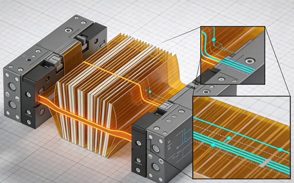
In the realm of advanced printed circuit board (PCB) design, rigid-flex technology represents the pinnacle of three-dimensional packaging. By combining the stability of rigid FR4 boards with the dynamic flexibility of polyimide layers, engineers can eliminate bulky connectors, reduce weight, and fit intricate electronics into unconventional enclosures. However, as the demand for higher interconnect density grows, designers frequently face a critical mechanical hurdle: managing multiple flex layers within a single assembly.
When a standard multi-layer rigid-flex PCB is bent, the flex layers undergo varying degrees of stress. The layers on the inner radius of the bend are subjected to compression, while the layers on the outer radius experience tension. If all flex layers are manufactured to the same length, the inner layers will inevitably buckle and wrinkle, while the outer layers will stretch, potentially leading to copper trace fracture or delamination. To overcome this fundamental limitation of material physics, the PCB manufacturing industry developed a highly specialized fabrication technique known as the bookbinder rigid-flex PCB.
This comprehensive guide delves deeply into the mechanics of bookbinder rigid-flex PCBs. We will explore how they solve intricate length constraints, detail their primary engineering advantages, discuss the manufacturing challenges involved, and provide a step-by-step process for designing them effectively.
Table of Contents
Understanding the Bookbinder Rigid-Flex PCB Concept
The term “bookbinder” is directly derived from the physical structure of a traditional bound book. If you take a thick paperback book and bend it into a U-shape, you will immediately notice that the pages slide past one another at the unglued edge. The pages located on the outer curve of the bend must cover a significantly greater geometric distance than the pages on the inner curve. If you were to glue those pages together at both ends and then attempt to bend the book, the inner pages would aggressively buckle, crumple, and ultimately ruin the structural integrity of the book.
A standard rigid-flex printed circuit board with multiple, bonded flex layers acts exactly like that book glued at both ends. When forced into a tight bend radius during final product assembly, the physical constraints of identical layer lengths cause catastrophic mechanical failure. Learn more about IPC-A-610 Class 3: Strict Inspection Criteria for Mission-Critical PCBA.
A bookbinder rigid-flex PCB elegantly solves this physical problem by stagger-lengthening the flex layers. During the intricate design and manufacturing process, each successive flex layer moving outward from the bend’s center of radius is manufactured to be slightly longer than the one beneath it.
When the completed PCB assembly is installed and folded into its final configuration, the extra, pre-calculated length in the outer layers perfectly compensates for the increased circumference of the outer bend radius. As a result, all flex layers lay perfectly parallel and smooth throughout the entirety of the curve. This completely eliminates compressive buckling on the inner layers and neutralizes tensile stretching on the outer layers, ensuring long-term reliability. Learn more about Load Boards: ATE (Automated Test Equipment) PCB Design Constraints.
Key Engineering Advantages of Bookbinder Technology
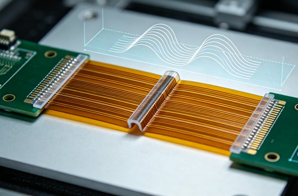
Implementing bookbinder technology in multi-layer rigid-flex designs introduces several significant advantages, particularly for mission-critical applications where mechanical reliability and extreme packaging density are paramount. Learn more about Semi-Flex PCBs: Cost-Effective Alternatives to Traditional Rigid-Flex Boards.
Total Elimination of Flex Layer Buckling and Stress
The primary, overriding function of the bookbinder configuration is to neutralize mechanical stress. By precisely calculating the required length for each individual flex layer, mechanical and electrical designers ensure that the dynamic forces of compression and tension are mitigated. This drastically increases the lifespan of the copper traces within the flex regions, preventing microscopic fractures that could lead to intermittent electrical failures, open circuits, or complete system breakdown in the field.
Enabling Significantly Tighter Bend Radii
Standard multi-layer flex designs are severely limited in their bending capabilities. IPC (Institute for Printed Circuits) guidelines typically restrict the safe bend radius of multi-layer flex to ten to twenty times their total combined thickness. Because the bookbinder method separates the flex layers into independent, unbonded ribbons within the flexible region, each layer acts individually rather than as a single thick composite mass. This allows for dramatically tighter bend radii, enabling denser packaging within confined spaces such as wearable medical devices or compact aerospace avionics housings.
Improved Signal Integrity and Impedance Control
In modern high-speed digital designs, maintaining precise impedance control across the entire signal path is absolutely essential. When standard flex layers buckle or delaminate due to bending stress, the physical distance and dielectric spacing between signal layers and their reference ground planes change unpredictably. This leads to severe impedance discontinuities, signal reflection, and overall signal degradation. The smooth, mathematically predictable geometry maintained by a correctly designed bookbinder layout ensures consistent dielectric spacing, thereby preserving delicate signal integrity across the flex transition.
Increased Airflow and Thermal Management
In high-power applications, standard bonded multi-layer flex circuits can trap heat. The unbonded nature of the flex ribbons in a bookbinder design allows for slight air gaps between the layers in the flex region. This can facilitate better convective cooling and thermal management, which is critical in densely packed, high-performance computing or military applications.
Applications of Bookbinder Rigid-Flex Boards
Due to the significantly increased manufacturing complexity, specialized tooling requirements, and overall cost, bookbinder rigid-flex PCBs are typically reserved for applications where space constraints and reliability requirements are extreme, and standard solutions are unviable.
- Aerospace and Defense: Avionics systems, missile guidance platforms, and satellite communications hardware require complex electronics to fit tightly inside curved or irregularly shaped housings. These systems must also withstand extreme vibration and thermal shock environments. Bookbinder designs provide the necessary reliability without the weight and volume penalty of mechanical connectors.
- Advanced Medical Devices: Surgical robotics, complex endoscopic equipment, and implantable electronic devices demand extreme miniaturization. The unique ability to fold multi-layer flex circuits into extremely tight spaces while maintaining high channel counts makes bookbinder technology ideal for these life-saving applications.
- High-End Consumer Electronics: Wearable augmented reality (AR) and virtual reality (VR) headsets utilize bookbinder designs to route hundreds of high-speed camera, sensor, and display signals across articulating hinges without succumbing to fatigue over the life of the product.
How to Design Bookbinder Rigid-Flex PCBs (Step-by-Step Guide)
Follow these engineering rules.
- Determine the Bend Radius and Flex Requirements
Begin by defining the strict mechanical constraints of the final product assembly. Determine the exact bend angle (e.g., 90 degrees, 180 degrees, or a custom angle) and the inner bend radius required to fit within the mechanical enclosure. Identify the total number of flex layers necessary to route all electrical signals and power planes. Ensure that the inner bend radius complies with IPC-2223 standards for the specific thickness of a single flex layer.
- Calculate the Progressive Length for Each Flex Layer
This is the most critical and mathematically demanding step in the bookbinder design process. You must calculate the exact added length required for each successive outer layer. The formula relies heavily on the bend angle, the inner bend radius, the thickness of the flexible laminates, and the spacing between the individual flex layers. A simplified mathematical approach for the added length (ΔL) per layer for a standard 180-degree bend is: `ΔL = π × (Thickness of flex layer + Air gap)`. For other bend angles, the added length is proportional to the fraction of a circle represented by the bend angle. These calculations must be exact to a tight tolerance; even a fraction of a millimeter of error can lead to buckling or tearing.
- Select the Appropriate Materials
Selecting the correct materials optimized for extreme flexibility and long-term dimensional stability is crucial. Adhesive-less polyimide copper clad laminates are strongly recommended, as traditional acrylic adhesives are prone to cracking under continuous stress and significantly increase the overall thickness of the flex layers. Use rolled annealed (RA) copper foil for the conductive traces in the flex region. You must mandate that the fabricator orients the grain direction of the RA copper parallel to the bending axis to maximize fatigue life and prevent micro-fracturing.
- Design the Transition Zones
The transition zone, the precise area where the flexible polyimide exits the rigid FR4 section, is the most mechanically vulnerable point of any rigid-flex PCB. Since the flex layers in a bookbinder design possess deliberately different lengths, the routing, via placement, and pad locations in the rigid sections must account for these dimensional offsets. Implement generous tear-drops on all trace-to-pad connections. Ensure that the polyimide coverlay and rigid prepreg are properly staggered to provide adequate strain relief at the rigid-flex interface, preventing stress concentrators.
- Prototype and Perform Mechanical Testing
Given the highly complex 3D geometry, a physical mechanical mock-up is essential before finalizing the electrical PCB layout. Create a “paper doll” or employ a specialized mechanical fabricator to laser-cut a rapid prototype from blank, unclad polyimide film. This physical model will allow you to verify the form, fit, and flex layer lengths within the actual physical enclosure. Once the mechanical fit is conclusively confirmed, proceed with full electrical prototyping and conduct rigorous environmental, thermal cycling, and mechanical bend testing to validate long-term product reliability.
Designing a bookbinder rigid-flex PCB is an incredibly complex process that demands close, continuous collaboration between the electrical engineer, the mechanical packaging engineer, and the chosen PCB manufacturer. Accurate calculations, material knowledge, and 3D modeling are non-negotiable prerequisites for success.
Manufacturing Challenges and Cost Implications
The fabrication of bookbinder rigid-flex PCBs is significantly more challenging than standard rigid-flex boards. This drastically limits the pool of PCB manufacturers capable of producing them reliably, and impacts the overall project budget. Learn more about SMT Stencil Design: Nano-Coating and Step-Stencils for Mixed Technology.
- Complex Lamination and Registration: Because the individual flex layers are intentionally designed to be different lengths, aligning them accurately during the lamination of the outer rigid FR4 sections requires highly specialized tooling, custom alignment pins, and unique fixturing. The progressively longer flex layers must be meticulously folded, bubbled, or otherwise accommodated within the lamination press platens to prevent damage under extreme heat and pressure.
- Etch Factor and Trace Tolerance Control: The precise mathematical length calculations assume exact, uniform material thicknesses. However, real-world variations in dielectric polyimide thickness, adhesive thickness, or copper plating variations can compound across multiple layers, throwing off the delicate bookbinder mechanics. Strict statistical process control (SPC) is required by the fabricator.
- Increased Cost: The absolute need for specialized lamination tooling, dramatically increased manual handling by skilled operators, slower throughput, and historically higher scrap rates makes bookbinder PCBs noticeably more expensive than standard rigid-flex assemblies. Engineering teams must carefully weigh this financial cost against the strict mechanical necessity of the design.
Conclusion
Bookbinder rigid-flex PCBs represent an incredibly elegant, albeit highly complex, engineering solution to the strict physical limitations of high-density multi-layer flex circuits. By conceptually mimicking the sliding pages of a bound book, this staggered-length technique entirely eliminates buckling, minimizes destructive stress on copper traces, and enables packaging densities previously thought physically impossible.
While the electrical and mechanical design phases, as well as the manufacturing processes, demand meticulous attention to microscopic detail and rigorous mathematical modeling, the resulting reliability makes bookbinder technology an invaluable asset. For engineering teams developing cutting-edge aerospace systems, advanced surgical robotics, and next-generation wearable defense electronics, mastering the bookbinder technique is essential for pushing the boundaries of what is possible in electronic packaging.
Frequently Asked Questions (FAQ)
A standard rigid-flex PCB features flex layers of completely identical lengths between the rigid sections. This limits the safe bend radius and causes buckling on inner layers and stretching on outer layers when bent. A bookbinder rigid-flex PCB utilizes staggered, differing flex layer lengths, with outer layers progressively longer than inner layers, allowing them all to bend smoothly together in parallel without buckling or stretching.
While theoretically possible for static “flex-to-install” applications, it is highly recommended to use rolled annealed (RA) copper for all bookbinder designs. RA copper possesses a distinct horizontal grain structure that, when oriented parallel to the axis of the bend, provides vastly superior resistance to fatigue and cracking compared to the vertical grain structure of ED copper.
Theoretically, there is no strict physical limit, but practical manufacturing constraints and yield considerations usually dictate a maximum. Most successful bookbinder designs feature between 3 and 8 distinct flex layers (which may each be single or double-sided). Beyond this number, the lamination, registration, and press compensation processes become prohibitively complex and expensive for most applications.
Bookbinder designs are primarily intended for static “flex-to-install” applications where the finished board is folded once into an enclosure during final assembly and remains in that position for its lifespan. While they perform exponentially better under bending stress than standard multi-layer flex, the complex mechanical transition zones are not typically designed to withstand the millions of continuous cycles required in true dynamic flex applications (like a printer head cable).
The increased cost is directly attributable to highly complex manufacturing requirements. Aligning and laminating internal layers of varying lengths requires specialized custom tooling, complex lamination press configurations, and significant manual handling by expert technicians. This leads to higher direct labor costs, longer fabrication times, and potentially lower manufacturing yields compared to standard, uniform-length rigid-flex fabrication.