PCBWay vs TOPFAST: Which PCB Manufacturer Is Better for Your Project?
A detailed comparison of PCBWay and TOPFAST covering PCB fabrication quality, PCBA services, engineering capability, certifications, pricing, and production scalability.

A detailed comparison of PCBWay and TOPFAST covering PCB fabrication quality, PCBA services, engineering capability, certifications, pricing, and production scalability.
A complete guide for engineers and buyers choosing a PCB manufacturer for prototypes, multilayer boards, HDI PCBs, and mass production.

A detailed comparison of the best PCB manufacturers in 2026, covering quality, pricing, delivery, certifications, and engineering capabilities.
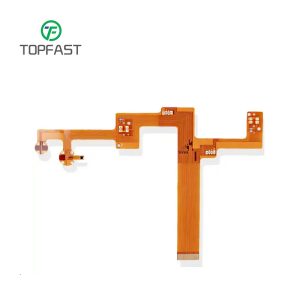
Telecommunication equipment requires PCB manufacturing with precise impedance control, signal integrity management, and stable production consistency. This article explains the…
Power and energy electronics require PCB manufacturing with exceptional thermal performance, electrical stability, and long-term reliability. This article explains the…
Industrial control systems require highly reliable and stable PCB manufacturing. This article explains the key requirements for an industrial control…
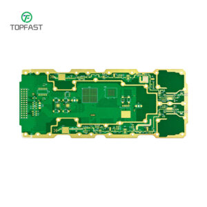
14 layer PCB boards are commonly used in AI hardware, telecom infrastructure, FPGA systems, and high-speed computing platforms. This guide…
12 layer PCB is widely used in FPGA systems, telecom equipment, industrial control, and high-speed embedded hardware. This article shares…

Medical electronics require exceptional reliability, traceability, and manufacturing consistency. This article explains the key requirements for a medical PCB factory,…
Looking for a reliable PCB manufacturer in 2026? Read our complete buyer's guide covering technical capabilities, quality certifications, and top…
Automotive electronics demand the highest levels of reliability, consistency, and compliance. This article explains what makes a PCB factory suitable…
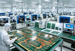
Quality control is one of the most critical factors in PCB manufacturing. This article explains how PCB factories ensure consistent…