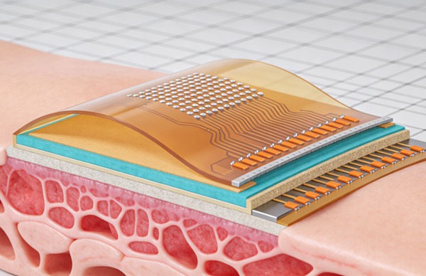
Table of Contents
Introduction to Biocompatible Printed Circuit Boards
The intersection of advanced electronics and biomedical engineering has ushered in a new era of active implantable medical devices (AIMDs). From cardiac pacemakers and implantable cardioverter-defibrillators (ICDs) to neuromodulation devices, cochlear implants, and continuous glucose monitors, the efficacy of these life-saving technologies hinges entirely on their foundational electronic infrastructure. Central to this infrastructure is the biocompatible Printed Circuit Board (PCB). Learn more about Probe Cards: Design and Manufacturing of Multi-Layer Test Interface Boards.
Unlike conventional commercial or industrial electronics, PCBs designed for implantation must operate flawlessly within the harsh, corrosive, and highly sensitive environment of the human body for years, or even decades, without failure. Any malfunction or degradation can result in catastrophic clinical consequences. Furthermore, the electronic components and the substrate itself must not elicit an adverse immune response, tissue toxicity, or chronic inflammation. Achieving this delicate balance requires highly specialized substrate materials, exotic conductive traces, and hermetic encapsulation techniques, pushing the boundaries of traditional PCB manufacturing. This article explores the cutting-edge materials and engineering methodologies required to produce highly reliable biocompatible PCBs.
Core Engineering Challenges in Implantable PCB Design
Designing PCBs for the human body presents a unique set of interdisciplinary challenges that require rigorous adherence to specialized engineering principles. These challenges dictate every aspect of the design and fabrication process.
Miniaturization and High-Density Interconnects (HDI)
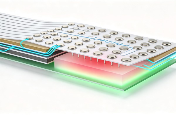
Implantable devices are subjected to stringent volumetric constraints. To minimize surgical invasiveness and patient discomfort, the form factor of the AIMD must be as small as physically possible. This necessitates the use of ultra-High-Density Interconnect (HDI) PCB technologies. Engineers must utilize microvias, blind and buried vias, and fine-pitch component placements. Trace widths and spacing often dip below 25 microns (1 mil). This extreme miniaturization complicates the fabrication process, requiring advanced laser drilling, sequential lamination, and stringent impedance control to ensure signal integrity across densely packed routing layers while maintaining sufficient dielectric spacing to prevent electromigration.
Thermal Management and Tissue Safety
Electronic components inherently dissipate power as heat during operation. In an implantable application, excessive localized heating can cause surrounding tissue damage, protein denaturation, or necrosis. Regulatory standards mandate that the surface temperature of an implant must not rise more than 1°C to 2°C above normal body temperature (approximately 37°C). Consequently, biocompatible PCB design must incorporate aggressive thermal management strategies. This includes the strategic placement of thermal vias, the use of substrates with optimized thermal conductivity, large copper pours for heat spreading, and the design of ultra-low-power integrated circuits (ICs) and microcontrollers to minimize total power dissipation at the source. Learn more about Cavity PCBs: Designing Recessed Cavities for RF Power Amplifiers.
Hermeticity and Fluid Ingress Prevention
The human body is an aggressive, conductive saline environment. If bodily fluids breach the PCB, the resulting ionic contamination will rapidly cause electrochemical migration, dendritic growth, and catastrophic short circuits. While the final device is typically housed in a hermetically sealed titanium enclosure, the PCB itself often requires secondary lines of defense, such as conformal coatings or encapsulation, to guarantee absolute reliability even if microscopic moisture permeation occurs over a 10-to-20-year operational lifespan.
Advanced Biocompatible Materials for PCBs
The selection of materials is the most critical phase in biocompatible PCB engineering. Standard FR-4 fiberglass and copper are generally unsuitable for direct tissue contact and long-term implantation due to rigidity, potential toxicity, and susceptibility to moisture absorption over long periods.
Flexible and Biocompatible Substrates
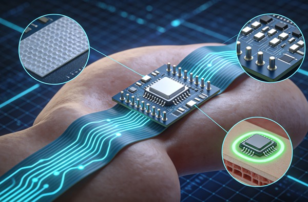
Rigid-flex and pure flexible circuits are predominantly used in AIMDs to conform to the anatomical contours of the body, maximize space utilization within the titanium can, and to withstand mechanical stress from patient movement.
* Liquid Crystal Polymer (LCP): LCP has emerged as a premier substrate for implantable PCBs. It boasts an extraordinarily low moisture absorption rate (typically <0.04%), excellent dielectric properties for high-frequency RF telemetry (crucial for wireless data transmission to external programmers and diagnostic equipment), and inherent biocompatibility. LCP can be thermoformed into complex 3D shapes, making it ideal for severely space-constrained enclosures.
* Polyimide (PI): Traditional polyimide remains a staple for flexible implantable circuits. While it has higher baseline moisture absorption than LCP, specialized medical-grade polyimides are engineered to mitigate this issue. PI offers exceptional thermal stability, extreme flexibility, and high tensile strength, making it suitable for dynamic applications like neural electrode arrays and pacing leads.
* Parylene C: While technically not a base substrate in the traditional sense, Parylene C is a critical material often used as a structural layer or a primary dielectric in ultra-thin, thin-film microelectrode arrays. It is vapor-deposited at room temperature, providing a completely pinhole-free, chemically inert, and highly biocompatible foundation.
Conductive Materials and Noble Metals
Standard bare copper is highly toxic to biological tissue and oxidizes rapidly in saline environments, leading to rapid electrical failure and adverse biological reactions. Therefore, conductive traces and pads on a biocompatible PCB must be carefully engineered, especially for any exposed sensing or stimulation nodes.
* Gold (Au) and Platinum (Pt): These noble metals are extensively used for exposed pads, electrode contacts, and sometimes entire trace runs in highly sensitive applications. They are chemically inert, highly conductive, and exhibit exceptional biocompatibility. Platinum-Iridium (Pt-Ir) alloys are frequently utilized for active stimulation electrodes due to their superior charge injection capacity, mechanical durability, and resistance to corrosion during electrical pulsing.
* Titanium (Ti): Often used as an adhesion layer (tie layer) between the polyimide or LCP substrate and the primary noble metal conductor (like gold or platinum). Titanium promotes excellent mechanical bonding, prevents delamination, and is itself highly biocompatible.
* ENIG and ENEPIG Surface Finishes: For components that will be hermetically sealed within a titanium can, Electroless Nickel Immersion Gold (ENIG) or Electroless Nickel Electroless Palladium Immersion Gold (ENEPIG) are standard surface finishes. They provide excellent solderability for high-density component mounting and wire bonding while preventing underlying copper migration.
Encapsulation and Conformal Coatings
To protect the populated PCB assembly from potential moisture ingress and to prevent the leaching of toxic ions, rigorous encapsulation at the board level is required, acting as a critical secondary barrier.
* Atomic Layer Deposition (ALD): ALD allows for the deposition of ultra-thin (nanometer scale), highly conformal films of ceramic materials like Aluminum Oxide (Al2O3) or Titanium Dioxide (TiO2). These nanoscale ceramic coatings provide unparalleled barriers against moisture and ion diffusion without adding significant volume or mass to the device.
* Medical-Grade Silicones and Epoxies: Specially formulated, USP Class VI certified silicones and epoxies are used for potting, underfilling, or localized encapsulation of sensitive components. These materials must be strictly evaluated for extractables and leachables to ensure no toxic byproducts, unreacted monomers, or catalysts are released into the body over time.
How to Design Biocompatible PCBs (Step-by-Step Guide)
Follow these engineering rules.
- Define the Physiological Operating Environment
Begin by meticulously documenting the specific anatomical location where the device will be implanted. Determine the mechanical stresses (flexion, torsion, compression), ambient temperature variations, exposure to specific body fluids (blood, cerebrospinal fluid, interstitial fluid), and the expected operational lifespan of the implant. This environmental profile dictates all subsequent material and design choices.
- Select the Appropriate Biocompatible Substrate
Based on the environmental profile, required form factor, and frequency requirements, choose the base material. Opt for Liquid Crystal Polymer (LCP) if ultra-low moisture absorption and high-frequency RF telemetry are paramount. Select medical-grade Polyimide if dynamic flexibility, high temperature resistance during fabrication, and complex rigid-flex topologies are required.
- Design High-Density Interconnects (HDI) for Miniaturization
Utilize advanced HDI design principles to shrink the PCB footprint to the absolute minimum. Implement staggered microvias, blind and buried vias, and any-layer via structures to optimize routing channels. Maintain strict design rules for trace widths and clearances, ensuring manufacturing tolerances are tightly controlled by the chosen medical PCB fabricator to prevent micro-shorts in ultra-dense layouts.
- Implement Robust Power and Thermal Management
Calculate the maximum power dissipation of all active components under worst-case operating conditions. Distribute high-power ICs across the board area to prevent localized thermal hotspots. Integrate thermal vias to conduct heat away from critical junctions and into the broader substrate or structural housing, ensuring the external tissue contact temperature remains strictly within the regulatory 1°C to 2°C threshold.
- Specify Hermetic Sealing and Encapsulation Techniques
Define the primary and secondary barriers against moisture and ionic contamination. Specify the surface finishes (e.g., ENEPIG) for optimal solderability and wire bonding reliability. Determine if the entire assembly requires an Atomic Layer Deposition (ALD) coating or Parylene C vapor deposition to serve as an absolute moisture barrier prior to final integration into the titanium device housing.
- Execute Rigorous Reliability and Biocompatibility Testing
Before finalizing the design for mass production, mandate a comprehensive suite of hardware tests. This includes Highly Accelerated Life Testing (HALT), severe temperature cycling, mechanical shock, and vibration testing. Most importantly, ensure the final assembled board undergoes ISO 10993 biocompatibility testing, specifically evaluating cytotoxicity, sensitization, and irritation based on potential extractables and leachables.
Designing a PCB for an implantable medical device requires a highly structured, risk-averse methodology that prioritizes reliability above all other metrics.
Regulatory Compliance and Quality Assurance
The manufacturing of biocompatible PCBs is governed by some of the strictest regulatory frameworks in the world, primarily overseen by the FDA (Food and Drug Administration) in the United States and the MDR (Medical Device Regulation) in the European Union. Most active implantable electronics fall under Class III medical devices, representing the highest risk category, where failure directly threatens human life.
Facilities producing these PCBs must operate under ISO 13485 certified Quality Management Systems (QMS). This standard demands exhaustive traceability of all raw materials down to the lot number, rigorous process validation (IQ/OQ/PQ), and comprehensive documentation of every manufacturing step. A single undocumented change in a solder paste formulation, a cleaning solvent, or a substrate batch can completely invalidate the entire device certification and require expensive recertification.
Furthermore, the materials used must be evaluated against the ISO 10993 series of standards, which assesses the biological evaluation of medical devices. This testing ensures that the materials do not produce systemic toxicity, genotoxicity, carcinogenicity, or adverse local tissue responses. Learn more about Bookbinder Rigid-Flex PCBs: Solving Length Constraints in Multi-Flex Layers.
The Future of Implantable PCB Technology
The trajectory of biocompatible PCBs is moving towards increasingly seamless integration with human biology. We are witnessing the advent of transient electronics—PCBs fabricated from biodegradable materials like magnesium, zinc, and specialized silk, PLA, or cellulose substrates. These devices are designed to perform a diagnostic or therapeutic function for a specific duration (e.g., monitoring post-surgical healing) and then harmlessly resorb into the body, eliminating the need for a secondary surgical extraction procedure. Learn more about RF PCB Design: Impedance Matching and Dielectric Loss Control with Rogers Materials.
Additionally, advancements in soft electronics and stretchable substrates using liquid metal alloys (like Galinstan) embedded in highly elastomeric polymers will yield PCBs that mimic the mechanical moduli of human tissue (such as skin, muscle, or nerve bundles). This will dramatically reduce the foreign body immune response, minimize fibrotic encapsulation, and enable chronic, high-resolution neural interfaces and advanced prosthetic control systems, forever blurring the line between synthetic electronics and organic tissue.
Frequently Asked Questions (FAQ)
Standard FR-4 contains rigid woven fiberglass and brominated epoxy resins that are not designed or certified for in vivo applications. FR-4 is highly rigid, potentially causing tissue trauma or shearing forces against soft tissue. Furthermore, its resins can leach toxic compounds over time. FR-4 also has a relatively high moisture absorption rate compared to LCP, which can lead to rapid electrical failure (like dendrite growth and short circuits) in the aggressive saline environment of the human body.
Biocompatibility refers to the ability of a material to exist within the body without provoking a toxic, immunological, inflammatory, or foreign-body response. It concerns the chemical and biological interaction with tissue. Hermeticity, on the other hand, refers to a physical seal that completely prevents the ingress of gases and liquids (like bodily fluids) into the electronic enclosure. A successful AIMD must typically use biocompatible materials on its exterior while maintaining absolute hermeticity to protect the internal, non-biocompatible electronics (like standard ICs and copper traces) from corrosion.
Engineers use ultra-low-power microcontrollers and carefully manage the active duty cycles of the device (putting the device to sleep whenever possible) to minimize total heat generation. On the PCB level, they utilize substrates with better thermal conductivity, design extensive copper pours as heat spreaders, and use thermal vias to distribute heat evenly across the entire surface area of the device. Regulatory standards strictly limit the surface temperature increase of an implant to prevent tissue necrosis and protein denaturation.
Parylene C is a highly utilized conformal coating deposited via chemical vapor deposition (CVD) in a vacuum at room temperature. It provides an exceptionally uniform, pinhole-free, and chemically inert layer that acts as a superb dielectric and moisture barrier, even over complex 3D topologies. Because it is highly biocompatible and biostable, it is often used to coat flexible neural probes, exposed sensor elements directly contacting tissue, and as a secondary protective layer over populated PCBs before they are hermetically sealed.
For medical PCBs requiring wire bonding—often necessary for connecting bare die components directly to the board to minimize volumetric space—Electroless Nickel Electroless Palladium Immersion Gold (ENEPIG) is highly recommended. ENEPIG provides a very flat surface, excellent solderability for standard SMT components, and superior wire bonding reliability (for both gold and aluminum wire) without the risk of “black pad” syndrome associated with standard ENIG finishes. The palladium layer acts as a highly effective barrier preventing nickel diffusion into the gold layer.