In the highly competitive realm of printed circuit board assembly (PCBA) manufacturing, ensuring the reliability and functionality of every board is paramount. A single manufacturing defect can lead to catastrophic system failures in the field, resulting in costly product recalls, warranty claims, and significant, long-lasting damage to a brand’s reputation. To mitigate these inherent risks, engineers and production managers must implement rigorous, robust testing methodologies at the end of the surface mount technology (SMT) line. Two of the most prominent and widely adopted electrical testing techniques in the electronics manufacturing industry are In-Circuit Testing (ICT) and Flying Probe Testing (FPT).
Both of these advanced testing strategies are specifically designed to detect common manufacturing defects that occur during the assembly process. These defects include solder shorts between adjacent pins, open circuits due to insufficient solder, incorrect component values installed by a pick-and-place machine, reversed polarities on capacitors and diodes, and entirely missing components. However, while their end goal is identical, ICT and FPT approach the task using fundamentally different mechanical architectures and software approaches.
Choosing between Flying Probe vs. ICT is never a simple matter of determining which technology is objectively superior. Rather, it requires a careful, nuanced analysis of your specific project requirements, with anticipated production volume, budget constraints, and printed circuit board complexity acting as the primary deciding factors.
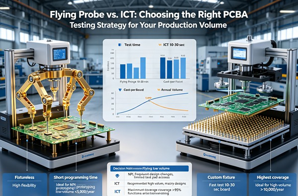
This comprehensive technical guide delves into the inner workings of both ICT and Flying Probe testing, objectively comparing their advantages, inherent limitations, cost structures, and ideal use cases. By understanding the capabilities of each, you will be well-equipped to formulate the optimal testing strategy for your unique manufacturing environment. Learn more about Conformal Coating: Protecting PCBA from Moisture, Dust, and Corrosive Environments.
Table of Contents
Understanding In-Circuit Testing (ICT)
In-Circuit Testing, commonly referred to in the industry as a “bed-of-nails” test, is a highly efficient, automated testing method used almost exclusively for high-volume production. An ICT system utilizes a custom-built, mechanically intricate test fixture containing hundreds or even thousands of spring-loaded pogo pins. When an assembled PCBA is placed into the fixture and the system is engaged—usually via a powerful vacuum system or a pneumatic mechanical press—these pogo pins make simultaneous, reliable contact with predetermined test points, vias, and component leads distributed across the entire bottom (and sometimes top) surface of the board. Learn more about Return Path Optimization: Designing Solid Reference Planes for High-Frequency Signal Integrity.
Once physical contact is firmly established, the ICT machine’s internal electronics execute a rapid sequence of precise electrical measurements. Because the system can access all necessary electrical nodes simultaneously, it leverages a technique called “guarding” to electrically isolate individual components from the rest of the complex circuit. This allows the machine to verify precise component values (resistance, capacitance, inductance) and detect structural assembly flaws with high accuracy.
Advantages of ICT
- Unmatched Speed and Throughput: The simultaneous, parallel connection allows an ICT system to completely test a complex, highly populated board in a matter of seconds. For high-volume manufacturing (HVM) facilities, this rapid throughput is absolutely critical to meeting aggressive production quotas without creating bottlenecks.
- Comprehensive Fault Coverage: ICT excels at identifying a wide array of manufacturing defects with pinpoint accuracy. Furthermore, many modern ICT systems can power up the board to perform limited functional testing, verifying the operation of specific analog circuits, relays, and digital logic gates.
- Consistency and Reliability: The rigid, fixed nature of the custom bed-of-nails fixture ensures highly repeatable and reliable test results across tens of thousands of manufactured boards, minimizing false calls and ensuring consistent quality control.
Limitations of ICT
- Exorbitant Upfront Costs: Designing, routing, and mechanically fabricating a custom test fixture for each specific PCBA revision is an expensive and time-consuming endeavor. Tooling costs can easily exceed tens of thousands of dollars for complex boards.
- Rigid Inflexibility: If the board layout changes even slightly—such as moving a test point by a few millimeters during a minor design revision—the existing ICT fixture becomes obsolete, necessitating the costly modification or complete recreation of the fixture.
- Strict Physical Space Requirements: As PCBA density increases and consumer electronics demand miniaturization, finding sufficient physical space to place hundreds of test pads can be incredibly challenging for PCB layout engineers.
Understanding Flying Probe Testing (FPT)
Flying Probe Testing is a highly flexible, entirely fixtureless automated testing method. Instead of relying on a massive, custom bed-of-nails, an FPT machine utilizes a small number (typically between four and eight) of highly precise, software-controlled electromechanical probes. These needle-like probes “fly” rapidly across the surface of the PCBA, moving from test point to test point in a coordinated ballet to take sequential electrical measurements. Learn more about Hard Gold Plating: Edge Connectors and Switch Contacts Design for Extreme Wear Resistance.
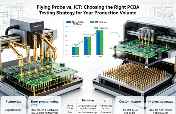
The intricate movement and targeting of these probes are dictated entirely by a test program generated directly from the board’s native CAD data, Bill of Materials (BOM), and Gerber files. This completely eliminates the need for any custom mechanical fixturing, making FPT highly adaptable to an infinite variety of board designs.
Advantages of Flying Probe Testing
- Zero Fixture Costs (Zero NRE): Because it is completely fixtureless, FPT eliminates the massive Non-Recurring Engineering (NRE) capital expenditure associated with designing and building ICT fixtures. You only pay for the programming time.
- Exceptional Flexibility and Agility: Test programs can be generated, refined, and debugged entirely in software within a matter of hours. If a board undergoes a sudden design revision, updating the FPT program to accommodate the new layout is quick and virtually cost-free.
- Ideal for High-Density, Miniaturized Boards: The highly articulated, microscopic probes can target extremely small test pads, vias, and even component legs directly on densely populated boards where traditional ICT pogo pins simply cannot fit due to pitch constraints.
- Rapid Setup and Time-to-Market: Transitioning a brand-new product design into the testing phase is much faster with FPT, accelerating the overall time-to-market for initial prototypes and pilot runs.
Limitations of Flying Probe Testing
- Significantly Slower Test Times: Because the limited number of probes must physically traverse the board and move sequentially between thousands of test points, testing a single complex board can take anywhere from a few minutes to well over an hour.
- Economically Unviable for High Volume: The inherently slow throughput makes FPT economically impractical for mass production runs where thousands of boards must be tested and shipped daily.
Key Differences: Flying Probe vs. ICT
To make a truly informed, strategic decision between these two testing methodologies, engineering managers must understand how they compare across several critical manufacturing vectors.
Cost Dynamics and Amortization
The cost models for ICT and FPT are perfectly inverted. ICT requires a massive initial capital investment in custom fixtures and complex programming, but the per-board testing cost is practically negligible due to the blazing speed. The upfront cost is easily amortized over a large production run. Conversely, FPT boasts almost zero upfront tooling costs, but the slow, sequential testing speed results in a significantly higher per-board testing cost. Therefore, the cost-effectiveness of each method hinges almost entirely on the projected production volume over the life of the product. Learn more about Skew Compensation: Managing Fiber Weave Effect (FWE) and Length Matching for PCIe Gen 6.
Programming and Setup Lead Times
Developing a robust ICT program and physically manufacturing the associated fixture can take anywhere from 4 to 8 weeks, requiring significant coordination with external fixture vendors. This long lead time must be aggressively factored into the product launch schedule. In stark contrast, an FPT program can be generated from CAD data, verified, and debugged in a single business day, making it the clear winner for rapid prototyping and agile manufacturing environments.
Testing Speed and Production Throughput
ICT is the undisputed champion of throughput. A moderately complex server motherboard that takes 15 minutes to fully test on a Flying Probe machine might be completely verified in just 30 to 45 seconds on a modern ICT machine. When manufacturing tens of thousands of units for global distribution, ICT is the only practical solution to prevent a catastrophic bottleneck at the quality assurance station.
Board Complexity and Component Density
Modern electronics, driven by the IoT and mobile device sectors, are pushing PCBAs to become increasingly dense, utilizing microscopic 01005 components and leaving minimal available real estate for dedicated test points. Flying probe machines, with their high-precision needle probes and advanced camera alignment systems, are vastly better equipped to handle these ultra-dense layouts. ICT fixtures struggle significantly when test points are too close together, as the physical pogo pins require a strict minimum pitch spacing (usually around 39 to 50 mils) to avoid physically colliding and shorting against each other.
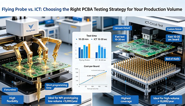
How to Choose the Right PCBA Testing Strategy (Step-by-Step Guide)
Follow these engineering rules.
- Assess Your Production Volume
The most critical factor in your decision matrix is the anticipated production volume. If you are manufacturing initial prototypes, low-volume pilot runs (NPI), or operating in a high-mix/low-volume (HMLV) contract manufacturing environment, Flying Probe is undoubtedly the economical choice. If your production run is guaranteed to exceed several thousand units (High-Volume Manufacturing), the speed of ICT becomes an absolute operational necessity to maintain throughput.
- Evaluate Board Complexity and Density
Review the PCBA layout meticulously with your design and layout team. Are there enough accessible test points for an ICT bed-of-nails? Are the components tightly packed? If the board is exceptionally dense, miniaturized, and lacks adequate test point spacing, creating an ICT fixture may be physically impossible or prohibitively expensive due to the need for specialized ultra-fine-pitch probes. In such scenarios, Flying Probe testing may be your only viable option.
- Analyze Your Budget and Upfront Costs
Examine your available capital expenditure (CapEx) budget for the new product introduction. ICT fixtures can cost anywhere from $5,000 for simple boards to well over $20,000 for complex, dual-sided boards requiring vacuum actuation. If your budget is tight, or if the product’s projected profit margins do not support amortizing that massive tooling cost over the expected volume, Flying Probe provides a risk-free, zero-capex entry point into high-quality electrical testing.
- Consider the Product Lifecycle and Revision Frequency
How stable is your product design? If you anticipate frequent design revisions, alternative component substitutions due to supply chain issues, or layout adjustments during the product’s lifecycle, an ICT fixture will become a constant financial drain, as every minor change requires a fixture modification. Flying Probe testing excels in dynamic, ever-changing environments because test programs can be updated via software in minutes.
- Determine Your Go-to-Market Timeline
If your company is under intense, competitive pressure to bring a new product to market immediately, the standard 4-8 week lead time required to build an ICT fixture may be completely unacceptable to stakeholders. Flying Probe testing allows you to begin testing and validating initial production runs on day one, drastically accelerating your time-to-market and allowing you to capture early market share.
Selecting the optimal testing strategy is not a guessing game; it requires a structured, analytical evaluation of your project’s specific parameters. Follow these steps to determine whether Flying Probe or ICT is the right choice for your PCBA manufacturing process.
The Hybrid Approach: Combining Both Strategies
In many modern manufacturing scenarios, the best approach is not choosing one over the other, but leveraging both at different stages of the product lifecycle. During the New Product Introduction (NPI) phase, an OEM might utilize Flying Probe testing for the first few batches (e.g., the first 500 units) to validate the design, catch early manufacturing defects, and verify the BOM without investing in expensive tooling. Once the design is officially locked down, proven stable, and volume is ready to ramp up into the thousands, the engineering team transitions the product to an ICT platform for long-term mass production. This hybrid strategy offers the best of both worlds: early agility and long-term efficiency.
Frequently Asked Questions (FAQ)
No, Flying Probe cannot completely replace ICT in high-volume manufacturing environments. While FPT is highly flexible, requires zero fixturing, and is cost-effective for low volumes, its sequential point-to-point testing method is far too slow to keep up with the rigorous throughput demands of mass production lines. ICT remains strictly essential for manufacturing electronics at scale.
Both methods offer excellent, highly reliable fault coverage for standard manufacturing defects (shorts, opens, missing components, wrong values). However, ICT generally provides slightly deeper coverage because it can often power up the board and perform limited functional testing on specific ICs, relays, and analog components, whereas FPT is primarily limited to unpowered impedance, capacitance, and parametric measurements.
Yes, this is a highly recommended strategy known as a hybrid approach. During the NPI phase, manufacturers use Flying Probe testing for initial batches to validate the design without tooling costs. Once the board design is finalized and volume ramps up, they invest in an ICT fixture for mass production.
Boundary scan (JTAG) is an advanced test methodology often used in conjunction with both ICT and FPT. Boundary scan tests the hidden interconnections beneath complex digital ICs (like BGAs, microprocessors, and FPGAs) without needing physical probe access to the pins. Modern ICT and Flying Probe machines can be equipped with hardware and software to execute boundary scan tests, significantly augmenting their physical probing capabilities.
If an EOL component is replaced by an alternative part with a completely different physical footprint, the existing ICT fixture will likely require physical modification by the vendor. If the required modification is extensive or impacts adjacent guard pins, a completely new fixture may need to be fabricated. This scenario highlights the inherent inflexibility of ICT compared to software-driven FPT.