Table of Contents
Introduction to Hard Gold Plating in PCB Design
When designing printed circuit boards (PCBs) for high-reliability applications, surface finish selection is one of the most critical decisions an engineer must make. While Electroless Nickel Immersion Gold (ENIG) provides an excellent coplanar surface for soldering surface-mount components, it is fundamentally unsuitable for sliding contact applications. For edge connectors (commonly known as gold fingers), rotary switches, slip rings, and membrane switch contacts that must endure repeated mechanical friction, hard gold plating is the undisputed industry standard.
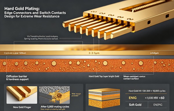
Hard gold, unlike its soft, pure gold counterpart, is an electroplated alloy specifically engineered to resist abrasive wear, fretting, and environmental degradation over thousands—or even tens of thousands—of insertion and wiping cycles. By codepositing gold with a hardening agent such as cobalt, nickel, or iron, the resulting metallurgical structure achieves exceptional durability while maintaining the superb electrical conductivity and oxidation resistance that make gold an ideal contact material.
This article explores the technical characteristics of hard gold plating, outlines critical design constraints for edge connectors and switch contacts, and provides a rigorous methodology for engineering highly reliable, wear-resistant sliding interfaces.
The Metallurgy and Material Properties of Hard Gold
To understand why hard gold is necessary for high-wear applications, one must examine its metallurgical properties. Pure gold (often referred to as soft gold) is highly ductile and has a Knoop hardness of roughly 60-90 HK25. If subjected to a sliding mating cycle, soft gold will gall, smear, and rapidly wear through to the underlying base metal, exposing it to oxidation and galvanic corrosion.
Hard gold is formulated as an alloy, typically consisting of 99.7% gold and 0.3% cobalt or nickel. This minute addition of a hardening element profoundly alters the microcrystalline structure of the deposit. The resulting alloy exhibits a Knoop hardness ranging from 130 to 200 HK25, significantly improving its resistance to abrasive and adhesive wear. Learn more about M-SAP Technology: Achieving Sub-25 Micron Line/Space for Next-Generation Electronics.
However, this increased hardness comes with trade-offs. The inclusion of cobalt or nickel increases the electrical resistivity of the finish slightly compared to pure gold, although it remains well within acceptable limits for most low-voltage, low-current signaling applications. More importantly, hard gold is generally not recommended for wire bonding or heavy soldering applications. The hardening elements can migrate during thermal excursions, leading to embrittlement of the solder joint (a phenomenon known as black pad or gold embrittlement if the thickness exceeds certain thresholds). Therefore, hard gold is selectively plated only on the areas requiring wear resistance.
The Critical Role of the Nickel Underplate
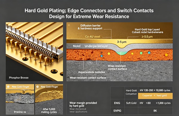
Hard gold is never plated directly over bare copper. A robust electrolytic nickel underplate is mandatory. This nickel layer, typically specified between 100 to 200 microinches (2.54 to 5.08 micrometers), serves three distinct and critical engineering functions:
1. Diffusion Barrier: At elevated temperatures or over extended periods, copper atoms can migrate into the gold layer, reaching the surface and oxidizing, which degrades contact resistance. The nickel layer acts as an impenetrable barrier to copper diffusion.
2. Load-Bearing Foundation: Hard gold is relatively thin. If placed directly over soft copper, the localized pressure from a mating connector pin could cause the copper to yield, cracking the hard gold layer (the “thin ice on mud” effect). The harder nickel provides a rigid mechanical substrate that supports the gold layer under compressive loads.
3. Pore Sealing: By providing a continuous, passive layer beneath the gold, the nickel prevents environmental corrosive agents from reaching the copper through any microscopic pores in the gold deposit.
Engineering Edge Connectors (Gold Fingers)
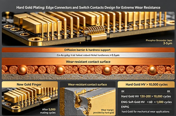
Edge connectors are the most common application for hard gold plating on PCBs. Used in memory modules (RAM), PCI/PCIe expansion cards, and industrial plug-in modules, these connectors must withstand repeated insertion and extraction forces against spring-loaded mating pins.
When designing edge connectors, the primary failure mechanisms to mitigate are abrasive wear (loss of plating thickness due to friction) and adhesive wear (galling). The design must also account for the mechanical tolerances of the mating receptacle and the electrical requirements of the signals passing through the interface.
Plating Thickness Specifications
The required thickness of the hard gold layer is directly proportional to the anticipated lifecycle (number of mating cycles) of the product. The IPC-4526 standard provides guidance on these specifications. Common thickness tiers include:
– 3-5 microinches (Flash Gold): Suitable only for very low cycle applications (fewer than 50 insertions), primarily used as a temporary environmental protectant rather than a true wear surface.
– 10-15 microinches: Standard commercial grade, adequate for up to 500 mating cycles. Commonly used in consumer electronics where parts are rarely swapped after initial assembly.
– 30 microinches (Class 2/3): The standard for industrial, telecom, and enterprise hardware. Capable of surviving 1000+ insertion cycles. This is the baseline recommendation for any high-reliability edge connector.
– 50+ microinches (Mil-Spec / Aerospace): Reserved for extreme environments, heavy wipe contacts, and life-critical applications subjected to severe vibration and fretting.
Current Carrying Capacity and Contact Resistance
Edge connectors must maintain a low and stable contact resistance, typically in the milliohm range. As the gold layer wears, or if debris accumulates in the mating interface, contact resistance increases, leading to localized I2R heating. When routing power through gold fingers, it is essential to distribute the current across multiple adjacent fingers to prevent thermal degradation of the fiberglass substrate (FR4) beneath the pads.
Engineering Switch Contacts for Extreme Wear
Beyond edge connectors, hard gold is heavily utilized in PCB-level switch mechanisms. These include membrane switches with metal snap domes, rotary encoders, sliding potentiometers, and elastomeric carbon-pill keypads.
Dome Switch Contacts
In a dome switch array, a stainless steel dome collapses to bridge two concentric hard gold-plated traces on the PCB. The failure mechanism here is typically not lateral abrasion, but rather compressive fretting wear caused by the microscopic scrubbing action of the dome feet as they flex downward. To maximize the lifespan of these contacts, the hard gold plating must be completely smooth and free of nodules. The traces should be designed to maximize the contact area with the dome feet, distributing the mechanical load.
Rotary and Sliding Contacts
For rotary switches and slip rings, the wiping action is continuous and severe. The mating wiper (often a beryllium copper alloy) exerts a high normal force to break through any superficial films or dust. In these designs, the hard gold plating thickness must be maximized (often 50 microinches or more). Additionally, the surface topography is critical. The traces should be oriented parallel to the wiping direction wherever possible to prevent the wiper from “bumping” over trace edges, which accelerates wear and generates conductive debris. Lubricants are sometimes employed in conjunction with hard gold to reduce the coefficient of friction and extend operational life.
How to Implement Hard Gold Plating (Step-by-Step Guide)
Follow these engineering rules. Learn more about Precision Impedance Control: How to Achieve ±5% Impedance Tolerance in High-Speed PCBs.
- Define Wear Requirements and Plating Thickness
Begin by explicitly defining the operational lifecycle of your product. Calculate the maximum number of mating cycles or switch actuations the board will endure. Consult IPC standards to determine the necessary gold thickness. For a standard PCIe card, specify 30 microinches (0.76 µm) of hard gold. Document this requirement clearly on your fabrication drawing and drill/fab notes, e.g., “Edge connectors to be plated with hard gold (99.7% Au, 0.3% Co), minimum thickness 30 microinches.”
- Specify the Nickel Underplate
Never omit the nickel specification. Ensure your fabrication notes dictate a robust electrolytic nickel barrier. The standard callout should read: “Electrolytic nickel underplate, minimum thickness 150 microinches (3.81 µm), to be applied under all hard gold surfaces.” This guarantees the necessary mechanical support and prevents copper migration.
- Route Tie-Bars for Electroplating
Because hard gold is electrodeposited, every pad receiving the plating must be electrically tied to a common cathode bus during the fabrication process. As a PCB designer, you must route small trace extensions (tie-bars) from the bottom edge of every gold finger out to the board outline. During manufacturing, these tie-bars connect to a temporary plating bus located in the panel margins. After the plating process is complete, the board is routed or v-scored, physically severing the tie-bars and electrically isolating the fingers. Ensure your design rules permit these traces to cross the board edge.
- Incorporate Chamfering for Edge Connectors
To prevent the sharp leading edge of the PCB from plowing into and damaging the mating connector pins during insertion, the board edge must be beveled (chamfered). On your fabrication drawing, define the angle and depth of the chamfer. The industry standard is typically a 20-degree to 45-degree bevel, cutting back into the board by a specified distance (e.g., 0.020 inches). Specify that the chamfering operation must occur *after* the hard gold plating process, but ensure that the resulting bare fiberglass edge does not expose copper from internal planes.
- Define Masking Requirements
Hard gold is expensive and should only be applied where necessary. The fabricator must apply a protective plater’s tape or a specialized photoresist over the rest of the board to prevent gold deposition in unintended areas. Clearly denote the boundaries of the hard gold area on a dedicated documentation layer in your Gerber or ODB++ files. Ensure that the soldermask layer is pulled back sufficiently from the gold fingers to allow the plater’s tape to seal tightly against the bare FR4, preventing plating bleed.
Properly implementing hard gold requires careful collaboration between the PCB designer and the fabrication house. Because hard gold is an electrolytic process, it requires a continuous electrical connection to all target pads during manufacturing. Follow these precise steps to ensure successful integration into your design.
Mitigation of Contamination and Failure Analysis
Even perfectly designed hard gold contacts can fail if not properly manufactured and handled. Plating bath contamination can lead to high porosity, allowing corrosive gases (such as sulfur dioxide or chlorine) to attack the underlying nickel, resulting in non-conductive corrosion products creeping onto the gold surface. Learn more about Flying Probe vs. ICT: Choosing the Right PCBA Testing Strategy for Your Production Volume.
During assembly, extreme care must be taken to prevent flux splatter, conformal coating, or silicon outgassing from contaminating the gold surfaces. A simple fingerprint contains enough organic oils and salts to drastically alter the contact resistance of a low-voltage switch. Handling protocols should mandate the use of cleanroom gloves and dedicated ESD packaging.
When failures do occur, they are typically analyzed using Scanning Electron Microscopy (SEM) combined with Energy Dispersive X-ray Spectroscopy (EDS). These tools can verify the plating thickness, inspect for micro-cracking in the nickel layer, and identify foreign contaminants that may be increasing contact resistance.
Frequently Asked Questions (FAQ)
While it is technically possible to solder to hard gold, it is highly discouraged. The cobalt or nickel alloying agents in hard gold interfere with the formation of a reliable intermetallic bond with the solder. Furthermore, the thickness of hard gold (often 30+ microinches) can lead to gold embrittlement in the solder joint, causing premature mechanical failure under stress or thermal cycling. Use ENIG or HASL for soldering, and restrict hard gold strictly to sliding contact areas.
ENIG (Electroless Nickel Immersion Gold) is a chemical deposition process that yields a very thin layer (typically 1-2 microinches) of pure, soft gold over nickel. It is designed primarily to protect the nickel from oxidation until the board is soldered. Hard Gold is an electrolytic process that deposits a much thicker, harder alloy of gold and cobalt/nickel, designed specifically to withstand repeated mechanical wear and friction.
When specifying a chamfer (bevel) on an edge connector, the routing bit cuts away the top and bottom edges of the PCB substrate. If internal copper planes extend into this chamfered zone, they will be exposed, creating a severe risk of electrical shorting to the mating connector’s pins. You must set appropriate keep-out zones for all internal layers, pulling planes and traces far enough back from the board edge to ensure they remain safely encapsulated in FR4 after the chamfering process.
Yes, this is a very common requirement known as Selective Gold Plating. The fabrication process becomes more complex and expensive, as it requires multiple masking and stripping steps. The fabricator will typically electroplate the hard gold fingers first, mask them off, and then process the rest of the board through the standard ENIG chemical baths. Be sure to clearly denote which surface finish applies to which features on your fabrication drawing.
Hard gold requires an electrolytic process, meaning a continuous electrical current must flow through every pad being plated. Tie-bars provide the conductive path from the pads to the external plating bus. If you forget to include them, the fabricator will not be able to plate the fingers using standard electrolytic methods. While electroless hard gold processes exist, they are rare, extremely expensive, and generally cannot achieve the thickness or hardness required for high-wear applications. Always route tie-bars to the board edge for edge connectors.