Table of Contents
Introduction to Press-Fit Technology
In the demanding field of printed circuit board assembly (PCBA), engineers are continually seeking methods to improve reliability, reduce manufacturing costs, and enhance the performance of electronic systems. Press-fit technology has emerged as a cornerstone for creating robust, solderless interconnects in high-reliability applications ranging from automotive electronics to telecommunications infrastructure. Unlike traditional through-hole technology (THT) or surface mount technology (SMT) that rely on solder alloys to establish electrical and mechanical bonds, press-fit connectors utilize mechanical deformation to achieve a gas-tight, highly conductive interface.
Understanding the mechanics of press-fit connectors and the stringent PCB manufacturing tolerances they require is critical for any hardware engineer or PCB designer. This article explores the principles of press-fit technology, the critical role of PCB hole tolerances, plating considerations, and the advantages of adopting solderless interconnects in modern electronic assemblies.
The Mechanics of Press-Fit Connectors
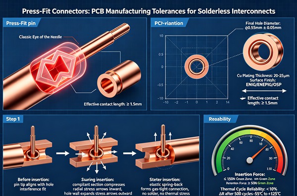
At its core, a press-fit connector consists of pins (or terminals) designed to be inserted into plated through-holes (PTH) on a printed circuit board. The pin features a compliant section—often resembling a needle’s eye, a “C” shape, or a localized bulge—that is slightly larger than the diameter of the PTH.
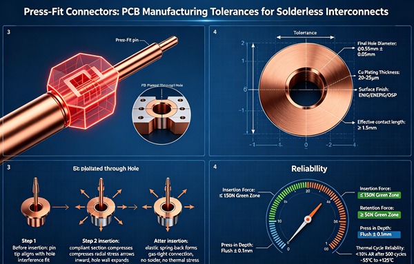
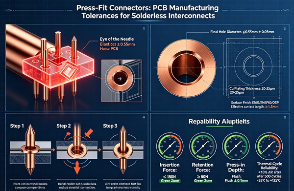
During the insertion process, specialized tooling applies a controlled force to press the connector pin into the hole. As the pin enters the PTH, the compliant section compresses elastically and plastically. This deformation exerts a continuous normal force against the walls of the plated through-hole. The resulting friction and pressure displace any oxides or contaminants on the contacting surfaces, creating a “cold weld” or gas-tight connection.
This gas-tight seal is impervious to moisture, corrosive gases, and environmental contaminants, ensuring long-term electrical stability. Furthermore, the absence of solder eliminates the risk of thermal stress during assembly, bridging, cold solder joints, and intermetallic embrittlement, making press-fit connections exceptionally resilient in high-vibration and high-temperature environments.
The Importance of PCB Manufacturing Tolerances
The reliability of a press-fit connection rests entirely on the precise mechanical interaction between the compliant pin and the plated through-hole. Consequently, PCB manufacturing tolerances are the most critical factor in the success of press-fit technology. If the hole is too large, the pin will not generate sufficient normal force, leading to a loose connection, increased contact resistance, and eventual failure. Conversely, if the hole is too small, the insertion force will be excessive, potentially buckling the pin, damaging the plating, or delaminating the PCB substrates.
To achieve the optimal balance, engineers must strictly adhere to the connector manufacturer’s specified tolerances for the finished hole size (FHS) and the drilled hole size (DHS).
Finished Hole Size (FHS) Tolerances
The finished hole size refers to the final diameter of the PTH after all plating processes have been completed. For press-fit applications, the FHS tolerance is typically extremely tight, often specified within ±0.05 mm (±2 mils) or even ±0.025 mm (±1 mil) for high-density connectors.
Maintaining this level of precision requires a highly controlled PCB manufacturing process. Fabricators must account for the thickness of the copper plating, as well as any surface finishes (such as ENIG, Immersion Tin, or HASL), when determining the initial drill size.
Drilled Hole Size (DHS) and Plating Thickness
The drilled hole size is the diameter of the hole cut into the bare FR-4 (or other dielectric) substrate before any plating occurs. The relationship between DHS, plating thickness, and FHS is given by:
FHS = DHS – (2 × Total Plating Thickness)
For press-fit holes, the copper plating thickness in the barrel of the hole is typically specified between 25 µm and 50 µm (1 to 2 mils). This robust copper layer provides the necessary structural integrity to withstand the insertion forces without tearing or cracking.
Fabricators must carefully control the drilling process to minimize runout, smear, and surface roughness inside the hole. High-quality carbide drill bits and optimized feed-and-speed rates are essential to produce smooth, perfectly cylindrical holes that ensure uniform plating distribution.
Surface Finishes for Press-Fit Interconnects
The surface finish applied to the PTH significantly impacts the insertion force, the quality of the cold weld, and the long-term reliability of the press-fit connection. Selecting the appropriate surface finish requires evaluating the specific requirements of the application and the connector material.
Immersion Tin (ImSn)
Immersion Tin is widely considered the optimal surface finish for press-fit applications, particularly in the automotive and telecommunications sectors. Tin provides excellent lubricity, reducing the required insertion force and minimizing wear on the pin. Furthermore, tin readily deforms under pressure, facilitating the creation of a large, highly conductive contact area. The characteristic thickness of ImSn is typically 0.8 µm to 1.2 µm.
Electroless Nickel Immersion Gold (ENIG)
ENIG offers superior corrosion resistance and a very flat surface, making it popular for high-reliability boards. However, nickel is a hard metal, which increases the insertion force compared to tin. Engineers using ENIG must ensure their press-fit equipment can deliver the necessary force without damaging the board or the connector. The typical ENIG finish consists of 3-6 µm of nickel and 0.05-0.12 µm of gold.
Hot Air Solder Leveling (HASL)
HASL and Lead-Free HASL are generally not recommended for press-fit connectors. The HASL process produces an uneven topography inside the PTH, making it nearly impossible to maintain the tight FHS tolerances required. The irregular surface can lead to inconsistent insertion forces and unreliable connections. Learn more about Return Path Optimization: Designing Solid Reference Planes for High-Frequency Signal Integrity.
Organic Solderability Preservative (OSP)
OSP provides a thin, organic coating that protects the copper from oxidation. While OSP can be used for press-fit applications, it requires careful handling. The insertion process easily breaches the OSP layer, establishing direct contact with the underlying copper. However, OSP offers no lubricity, meaning higher insertion forces are required. Learn more about Backdrilling: Eliminating Signal Reflection with Precise Controlled Depth Backdrilling.
Advantages of Solderless Interconnects
The shift towards press-fit technology is driven by several compelling engineering and manufacturing advantages over traditional soldered connections.
Thermal Stress Elimination
Soldering processes, particularly wave soldering and selective soldering, subject the PCB to extreme thermal excursions. This thermal shock can induce warpage, damage sensitive components, and compromise the integrity of multi-layer boards. Press-fit insertion is a purely mechanical, room-temperature process, completely eliminating thermal stress on the assembly.
Unmatched Reliability
The gas-tight interface of a press-fit connection is immune to the common failure modes associated with solder joints, such as cold soldering, voiding, flux entrapment, and fatigue cracking caused by coefficient of thermal expansion (CTE) mismatches. Press-fit connectors excel in environments subjected to severe shock, vibration, and thermal cycling. Learn more about Skew Compensation: Managing Fiber Weave Effect (FWE) and Length Matching for PCIe Gen 6.
Assembly Efficiency
Press-fit technology streamlines the PCBA manufacturing process. It eliminates the need for solder paste printing, reflow profiling, wave soldering setups, and post-assembly cleaning operations. This reduction in process steps translates to lower manufacturing costs, increased throughput, and higher overall yields. Learn more about Embedded Components: Miniaturizing IoT Devices with Embedded PCB Components.
Double-Sided Assembly Compatibility
In complex assemblies where components are densely packed on both sides of the board, routing a board through a wave soldering machine for THT components can be highly problematic. Press-fit connectors can be inserted after all SMT components have been reflowed on both sides, greatly simplifying the assembly sequence.
Repairability
While press-fit connections are highly permanent, specialized tooling allows for the safe extraction and replacement of damaged pins or connectors without the application of heat. This avoids thermal damage to the surrounding PCB area, a common risk when desoldering THT components.
How to Implement Press-Fit Technology (Step-by-Step Guide)
Follow these engineering rules.
- Select the Appropriate Connector
Begin by identifying a press-fit connector that meets the electrical (current, voltage, signal integrity) and environmental requirements of your application. Evaluate the pin design (e.g., eye-of-needle) and the manufacturer’s specified insertion force parameters.
- Define PCB Hole Specifications
Consult the connector manufacturer’s datasheet to determine the exact Finished Hole Size (FHS) and tolerance required. Typically, the tolerance is ±0.05 mm. Clearly document this requirement on the fabrication drawing.
- Specify Plating Thickness
Ensure the fabrication notes dictate the necessary copper plating thickness in the barrel of the hole, usually between 25 µm and 50 µm. This is critical for supporting the mechanical stress of insertion.
- Choose the Surface Finish
Select a surface finish compatible with press-fit technology. Immersion Tin (ImSn) is highly recommended for its lubricity, while ENIG is suitable for high-reliability applications. Explicitly prohibit HASL for the press-fit holes.
- Design the PCB Footprint
Create the PCB footprint according to the manufacturer’s recommendations. Ensure adequate annular ring size to prevent breakout during drilling and provide structural support during pin insertion.
- Communicate with the Fabricator
Share your design requirements with the PCB manufacturer early in the process. Confirm their capability to meet the tight drilling and plating tolerances required for the specified FHS.
- Plan the Assembly Process
Coordinate with the contract manufacturer (CM) or assembly facility to ensure they possess the appropriate press-fit insertion equipment. The tooling must support the PCB properly to prevent flexing and apply controlled, perpendicular force to seat the connector fully.
Successfully integrating press-fit connectors into a PCB design requires a systematic approach, from initial schematic capture to final assembly.
Best Practices for Press-Fit Assembly
The physical insertion of press-fit connectors is an exacting process that requires specialized equipment and meticulous setup.
Tooling and Support: The PCB must be uniformly supported from the bottom side using a custom fixture or anvil. This prevents board warpage or localized stress fractures during insertion. The upper tooling, or “press block,” must distribute the force evenly across the connector body, ensuring the pins enter the holes perfectly perpendicular to the board surface.
Force Monitoring: Modern press-fit equipment utilizes continuous force-distance monitoring. The system measures the force applied at every increment of insertion depth. This data generates a signature curve that is compared against predefined acceptable limits. If the insertion force is too low (indicating an oversized hole) or too high (indicating an undersized hole or misaligned pin), the machine alerts the operator, preventing defective assemblies from passing to the next stage.
Pin Standoff and Seating: Connectors must be pressed until they reach the manufacturer’s specified seating depth. Over-pressing can damage the PCB surface and the connector housing, while under-pressing compromises the electrical connection and the mechanical stability of the component.
Frequently Asked Questions (FAQ)
Yes, but with significant caveats. Flexible circuits generally lack the rigidity required to withstand insertion forces. Using press-fit connectors on FPCs typically requires the addition of stiffeners (such as thick FR-4 or polyimide layers) localized around the connector area to provide mechanical support.
Yes. Specialized extraction tools are available to pull press-fit pins or entire connectors out of the PCB without damaging the plated through-holes. Once removed, a new connector can typically be inserted into the same holes, although connector manufacturers usually recommend a maximum of two or three insertion cycles for a given hole to ensure the plating integrity remains intact.
Reliability testing typically involves environmental stress screening (ESS). This includes thermal cycling, damp heat testing, and random vibration testing. Following environmental exposure, the contact resistance of the press-fit joint is measured. An increase in contact resistance beyond a specified threshold (e.g., a change of greater than 10 milliohms) indicates a degradation of the gas-tight seal.
The Hot Air Solder Leveling (HASL) process results in an uneven distribution of solder inside the hole barrel, often creating a teardrop shape or varying thicknesses. This uneven topography makes it impossible to guarantee the tight diametrical tolerances (often ±0.05 mm) required for consistent and reliable press-fit insertion.
The Eye-of-the-Needle is the most common compliant pin design used in press-fit connectors. The center of the pin is split and bowed outward, resembling a needle’s eye. When inserted, the bowed sections compress inward, generating the continuous normal force required for the gas-tight connection while compensating for minor variations in the hole diameter.