The semiconductor industry is on a relentless pursuit of miniaturization, increased functionality, and higher processing speeds. As integrated circuits (ICs) become more complex, the packaging technologies housing them must evolve correspondingly. This evolution has led to a dramatic increase in pin counts and a significant reduction in pin pitch, particularly in packages like Ball Grid Arrays (BGAs), Chip Scale Packages (CSPs), and advanced System-in-Package (SiP) architectures. While these advancements offer unprecedented performance, they present formidable challenges during the critical phase of semiconductor reliability testing—specifically, burn-in testing.
Burn-in boards (BIBs) are specialized printed circuit boards (PCBs) designed to subject semiconductor devices to elevated temperatures and dynamic electrical stimulation over extended periods. This rigorous process is essential for weeding out “infant mortalities”—devices prone to early failure due to latent manufacturing defects. Designing burn-in boards for modern, high-pin count devices is a complex engineering endeavor. Traditional through-hole via (THV) PCB architectures simply cannot provide the routing density required to interface with hundreds or even thousands of closely spaced I/O pins. The solution lies in High-Density Interconnect (HDI) technology, leveraging the strategic implementation of blind and buried vias. Learn more about Dynamic Flex PCBs: Enhancing Bending Cycles in Wearable Devices.
This article delves into the technical intricacies of deploying blind and buried vias in burn-in boards, exploring their necessity, design considerations, and the profound impact they have on the efficacy of semiconductor reliability testing for high-pin count devices.
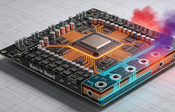
Table of Contents
The Challenge of High-Pin Count Devices in Burn-In Testing
In conventional burn-in testing, multiple devices under test (DUTs) are populated onto a single burn-in board to maximize throughput and minimize testing costs. Each DUT requires individual power, ground, and signal connections to the burn-in system’s stimulus and monitoring electronics.
When dealing with legacy components featuring low pin counts and wide pitches (e.g., DIP, SOIC), standard multilayer PCBs with mechanically drilled through-hole vias are sufficient. However, modern microprocessors, GPUs, and advanced memory modules frequently feature I/O counts exceeding 2,000 pins, with pitches shrinking below 0.5mm.
Attempting to route a burn-in board for such devices using only through-hole vias results in a routing nightmare. A through-hole via traverses the entire thickness of the PCB, consuming valuable routing real estate on every single layer, regardless of whether a connection is needed on that specific layer. In a densely populated burn-in board, the sheer volume of through-hole vias required to escape the BGA footprint (a process known as “breakout”) quickly exhausts the available routing channels. This forces designers to drastically increase the layer count of the PCB, leading to exorbitantly thick boards that are difficult to manufacture, exhibit poor signal integrity, and are prone to mechanical failure under the extreme thermal stresses of the burn-in oven. Learn more about Semi-Flex PCBs: Cost-Effective Alternatives to Traditional Rigid-Flex Boards.
Understanding Blind and Buried Vias in HDI PCBs
High-Density Interconnect (HDI) technology provides the essential toolkit for overcoming the limitations of traditional PCB design. HDI boards are characterized by finer lines and spaces, smaller capture pads, and, most importantly, microvias. Microvias are extremely small vias (typically less than 150 micrometers in diameter) formed using laser drilling technology rather than mechanical drills.
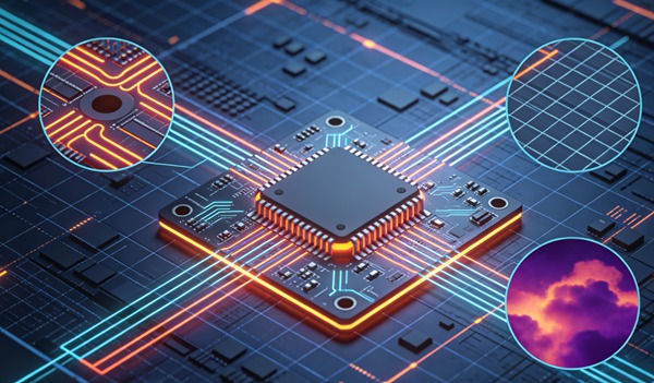
In the context of burn-in boards for high-pin count devices, the strategic use of blind and buried microvias is paramount. Learn more about Metal Core PCBs (MCPCB): Aluminum vs. Copper Base for High-Power LEDs.
- Blind Vias: A blind via connects an outer layer of the PCB to one or more inner layers but does not penetrate the entire board. Because they terminate within the substrate, blind vias free up routing space on the layers beneath them. They are primarily used for escaping dense BGA footprints on the surface layers, allowing signals to dive down to internal routing layers without obstructing the routing channels on the layers below.
- Buried Vias: A buried via connects two or more internal layers of the PCB and is entirely encapsulated within the board; it is not visible from either the top or bottom surface. Buried vias are highly effective for routing complex internal signal matrices and power/ground distribution networks without consuming space on the critical surface layers or other internal layers not involved in the connection.
Advantages of HDI Vias in Burn-In Boards
The integration of blind and buried vias transforms the architecture of burn-in boards, offering several critical engineering advantages when dealing with high-pin count devices.
Unprecedented Routing Density and Breakout Capability
The primary and most significant advantage is the exponential increase in routing density. By replacing space-consuming through-hole vias with microvias, designers can successfully break out thousands of signals from ultra-fine pitch BGAs. Blind vias allow signals to drop from the surface pads to internal layers precisely where needed, leaving the layers directly beneath free for other traces. This localized vertical interconnect architecture is the only viable method for routing highly complex, multi-DUT burn-in boards.
Controlled Layer Count and Board Thickness
Without HDI technology, routing high-pin count devices requires continuously adding internal signal layers. It is not uncommon for complex non-HDI designs to demand 30, 40, or even 50+ layers. Such thick boards (often exceeding 0.25 inches or 6.35mm) are incredibly difficult to fabricate reliably. The aspect ratio (the ratio of board thickness to drill diameter) for mechanically drilled through-holes becomes unmanageable, leading to plating failures and reliability issues. Furthermore, excessively thick boards act as massive thermal insulators, hindering the heat dissipation required during high-power burn-in testing.
Blind and buried vias optimize routing efficiency, allowing designers to drastically reduce the total layer count. A design that might require 40 layers using only through-hole technology can often be reduced to 20 or 24 layers using HDI techniques. This reduction in thickness improves manufacturability, reduces costs, and significantly enhances the board’s thermal profile.
Enhanced Signal Integrity and Electrical Performance
High-speed dynamic burn-in testing requires clean, undistorted signal transmission between the tester electronics and the DUTs. Through-hole vias act as electrical stubs—unterminated transmission line branches that cause signal reflections, impedance mismatches, and ringing at high frequencies.
Blind and buried vias virtually eliminate these parasitic stubs. Because a blind or buried via only spans the specific layers requiring connection, there is no excess via barrel projecting beyond the signal path. This structural characteristic significantly reduces parasitic capacitance and inductance, resulting in pristine signal integrity, tighter impedance control, and the ability to reliably transmit high-frequency test vectors. Learn more about IPC-A-610 Class 3: Strict Inspection Criteria for Mission-Critical PCBA.
Superior Thermal Management
During burn-in, semiconductor devices generate substantial heat that must be effectively managed to maintain precise junction temperatures and prevent catastrophic thermal runaway. The thermal conductivity of the PCB plays a vital role. HDI structures, while increasing electrical routing density, can also be leveraged for thermal management. Thermal microvias (often copper-filled) can be placed directly beneath the DUT dies or thermal pads to create highly efficient heat pipes, conducting thermal energy away from the device and into internal copper planes or external heat sinks.
Design and Engineering Considerations
While the benefits are profound, designing burn-in boards with blind and buried vias introduces significant engineering complexities.
- Material Selection: Burn-in boards operate in harsh environments, typically subjected to temperatures ranging from 125°C to 150°C (and sometimes higher) for hundreds of hours. The base laminate material must possess a high Glass Transition Temperature (Tg), low Coefficient of Thermal Expansion (CTE), and excellent thermal stability to prevent delamination, pad lifting, and via barrel cracking. High-performance polyimide or specialized high-Tg FR-4 blends are often mandatory.
- Sequential Lamination Cycles: Manufacturing PCBs with buried and blind vias requires sequential lamination. The board is built up in stages—drilling, plating, and laminating sub-assemblies before pressing them into the final composite structure. Each lamination cycle subjects the materials to immense heat and pressure, increasing manufacturing time, cost, and the potential for registration errors. Designers must optimize the layer stackup to minimize the number of lamination cycles required.
- Via Aspect Ratios: While laser-drilled microvias are small, they have strict aspect ratio limitations (typically a maximum of 1:1 or 0.8:1 depth-to-diameter). This means a microvia can usually only span one or two thin dielectric layers. Designers must carefully plan the “step-down” architecture, often stacking or staggering microvias to traverse multiple layers.
- Thermal Stress and Reliability: The repeated thermal cycling inherent in burn-in testing exerts massive stress on the copper plating within the vias due to the CTE mismatch between the copper and the dielectric substrate. Robust design practices, such as specifying adequate plating thickness, selecting low-Z-axis CTE materials, and employing stress-relieving via architectures (like staggered microvias instead of stacked, where applicable), are critical for long-term board reliability.
How to Design HDI Burn-In Boards for High-Pin Count Devices (Step-by-Step Guide)
Follow these engineering rules.
- Define Device and Test Requirements
Begin by thoroughly analyzing the Device Under Test (DUT). Document the exact package type, pin count, pin pitch, and power dissipation. Understand the specific burn-in parameters: maximum operating temperature, duration of the test, and the frequency/characteristics of the dynamic electrical signals required.
- Select Appropriate Board Materials
Based on the maximum burn-in temperature and the required board lifespan, select a suitable base laminate. High-Tg polyimide is the gold standard for high-temperature reliability, though advanced epoxy blends may suffice for lower temperature profiles. Ensure the chosen material has a low Z-axis CTE to minimize stress on the plated vias.
- Determine Stackup and Via Architecture
Collaborate closely with your PCB fabricator. Develop a layer stackup that accommodates the necessary routing density while minimizing sequential lamination cycles. Determine where blind vias are needed for BGA breakout and where buried vias can optimize internal routing. Establish the microvia aspect ratios and decide between stacked or staggered via configurations based on reliability requirements and manufacturer capabilities.
- Route High-Density Interconnects
Utilize advanced PCB design software capable of handling complex HDI rules. Focus first on the BGA breakout strategy using blind microvias. Ensure critical high-speed signals are routed on layers adjacent to solid reference planes and that via stubs are eliminated. Carefully manage power and ground distribution, utilizing buried vias to connect internal power islands without disrupting signal layers.
- Perform Thermal and Signal Integrity Simulation
Before finalization, run comprehensive thermal simulations to ensure the board can adequately dissipate the heat generated by the DUTs. Identify any hot spots and implement thermal microvia structures as needed. Concurrently, perform signal integrity (SI) simulations on critical high-speed traces to verify impedance matching, minimize crosstalk, and confirm that the blind/buried via transitions do not degrade the signal quality.
- Design for Manufacturability (DFM) Review
Conduct a rigorous DFM review with your chosen PCB manufacturer. Verify that all annular rings, drill sizes, spacing rules, and sequential lamination requirements align perfectly with their specific manufacturing capabilities and tolerances. An HDI burn-in board is only as good as its manufacturability.
Designing an HDI burn-in board is a rigorous process that demands meticulous planning and cross-functional collaboration.
Frequently Asked Questions (FAQ)
Mechanical drilling has physical limits. Drills smaller than 0.15mm (6 mils) are incredibly fragile, prone to breakage, and struggle to clear debris from the hole, leading to plating defects. Furthermore, the aspect ratio limits of mechanical drilling mean that a very small hole cannot penetrate a thick board reliably. Laser-drilled microvias solve these issues but are restricted to shallow depths, necessitating the blind/buried architecture.
Stacked microvias are placed directly on top of one another to traverse multiple layers vertically. Staggered microvias are offset from one another on adjacent layers. While stacked vias save more space, they create a solid column of copper that is highly susceptible to cracking under extreme thermal stress (like in a burn-in oven). For high-reliability burn-in boards, staggered microvias are generally preferred as they distribute the thermomechanical stress more evenly across the substrate.
Yes, the initial fabrication cost of an HDI PCB with sequential lamination, laser drilling, and specialized high-temperature materials is substantially higher than a standard through-hole board. However, for high-pin count devices, HDI is often the *only* technical solution. Furthermore, by enabling more DUTs per board (higher density) and reducing the overall layer count, HDI can sometimes lower the total cost of testing per device.
They generally improve it. Through-hole vias create parasitic stubs that cause signal reflection and degrade impedance control. Blind and buried vias only exist where the connection is required, eliminating these stubs. This allows for much cleaner signal transitions between layers, which is critical for dynamic burn-in testing involving high-frequency vectors.
No. Manufacturing HDI boards requires specialized equipment (laser drills, sequential lamination presses) and expertise. Manufacturing them using the high-temperature materials (like polyimide) required for burn-in boards adds another layer of complexity. It is crucial to partner with a PCB fabricator that explicitly specializes in both advanced HDI technology and high-reliability, high-temperature applications.