Table of Contents
The Evolution of High Density Interconnects in Modern Electronics
As electronic devices like flagship smartphones, augmented reality wearables, and implantable medical devices continue to shrink, traditional printed circuit board (PCB) routing techniques have hit a physical wall. There simply isn’t enough planar space to fan out high-pin-count BGA (Ball Grid Array) components using standard mechanically drilled through-holes.
This spatial bottleneck gave rise to High Density Interconnect (HDI) technology. However, even standard HDI (with structures like 1+N+1 or 2+N+2) sometimes falls short. Enter Any layer HDI PCB manufacturing—the absolute pinnacle of high-density routing. In this advanced technical guide, we will dissect the any-layer HDI architecture, analyze its manufacturing challenges, compare it to traditional HDI, and provide a roadmap for hardware engineers to integrate it successfully.

What is an Any Layer HDI PCB?
In a standard HDI board, microvias are typically limited to the outer layers, connecting layer 1 to layer 2 or layer 3. The inner “N” core is usually connected via a traditional, mechanically drilled buried via. This mechanical core takes up significant space and limits the routing density on the inner layers.

An Any-Layer HDI PCB (also known as Every Layer Interconnect or ELIC) eliminates the rigid mechanical core entirely. Instead, every single layer of the PCB is built up sequentially, and every layer can be connected to its adjacent layer using laser-drilled microvias. These microvias can be stacked directly on top of each other, creating a solid, copper-filled pillar that runs from any layer to any other layer—freely routing signals in three dimensions without occupying space on the layers in between.
Key Advantages of Any Layer HDI
- Ultimate Miniaturization: By eliminating large mechanical drills and via capture pads, you free up up to 40% more routing space. This allows for significantly smaller PCB form factors without sacrificing functionality.
- Superior Signal Integrity: Stacked, copper-filled microvias have significantly lower parasitic capacitance and inductance compared to traditional through-holes. This is vital for multi-gigabit signal transmission, which we cover extensively in Essential High Speed PCB Routing Techniques.
- High-Pin-Count BGA Support: It is the only viable way to route components with a pitch of 0.4mm or less without dropping signals or creating routing bottlenecks.
- Enhanced Reliability: Because microvias are much smaller and filled with solid copper, they are less prone to cracking under thermal stress compared to hollow, mechanically drilled vias.
Deep Dive: Stacked vs. Staggered Microvias
When designing an Any-Layer HDI board, you have two primary methods for transitioning between multiple layers: stacking or staggering microvias.
Stacked Microvias
Stacked microvias are aligned directly on top of one another.
Pros: Consumes the absolute minimum amount of spatial footprint. Offers the shortest possible electrical path, improving signal integrity.
Cons: Manufacturing is highly complex. The lower microvia must be perfectly filled with solid copper and planarized (flattened) before the next microvia can be laser-drilled and plated on top of it. Stacking more than three or four microvias introduces significant Z-axis thermal stress, increasing the risk of via separation during reflow soldering.
Staggered Microvias
Staggered microvias are offset from one another on adjacent layers.
Pros: Much easier to manufacture. The thermal stress is distributed across a wider area, drastically improving the mechanical reliability of the board during assembly and in the field.
Cons: Consumes more physical space on the PCB. The electrical path is slightly longer, which may have negligible impacts at extreme frequencies.
How to Design for Any Layer HDI (Step-by-Step Guide)
Follow these engineering rules.
- Consult the Fab House Early
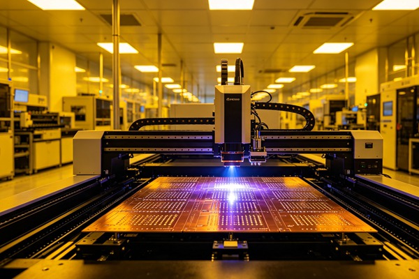
Any-layer HDI requires advanced Laser Direct Imaging (LDI) and sequential lamination. Confirm your manufacturer’s specific microvia aspect ratio limits (usually 0.8:1 or 1:1) and minimum dielectric thickness.
- Define the Via Stackup
Set up your CAD tool to allow blind and buried microvias across all adjacent layers. Define the rules for “Stacked Vias” versus “Staggered Vias” in your DRC (Design Rule Check).
- Prioritize Staggered Over Stacked
While stacked vias offer the shortest electrical path, limit stacking to 2 or 3 layers max to avoid severe thermal stress during reflow soldering. Whenever routing space allows, stagger your microvias.
- Implement Via-in-Pad
Route your microvias directly inside the BGA pads. Since these microvias must be solid copper-plated and planarized, they will not wick solder away during the assembly process, preventing weak solder joints.
- Utilize Resin Coated Copper (RCC)
Traditional prepreg contains fiberglass weaves that can deflect laser drills, causing non-circular holes. Specify RCC or specialized laser-drillable prepregs for the build-up layers to ensure clean, precise microvia formation.
Designing an any-layer HDI board requires a fundamental shift in how you approach your EDA (Electronic Design Automation) tool. Follow these steps to ensure manufacturability:
Overcoming Any Layer HDI Manufacturing Challenges
The transition to Any layer HDI PCB manufacturing is not without its hurdles. Yield rates are heavily dependent on the fabricator’s process control and capital equipment.
Copper Plating Voids
Filling blind microvias with solid copper without trapping air bubbles or chemical residues is highly complex. Advanced pulse plating chemistry is required. If a void forms inside the stacked via, it acts as a stress concentrator that will almost certainly crack during the high temperatures of the assembly process.
Registration Accuracy
Because the board is built up layer by layer in a sequential lamination process, maintaining alignment (registration) across 10 or 12 layers requires state-of-the-art optical alignment tools (LDI). A deviation of just 20 micrometers can cause a microvia to miss its target pad, ruining the entire board.
Surface Planarity
To stack a via, the surface beneath it must be perfectly flat. Manufacturers must employ chemical mechanical planarization (CMP) or specialized plating techniques to ensure the copper surface is completely smooth before the next dielectric layer is applied.
If your device operates in dynamic mechanical environments, you might also want to combine HDI techniques with flexible materials. Read our guide on Navigating Rigid Flex PCB Design Rules for more information.
Case Study: Implementing ELIC in Mobile Devices
Consider a modern 5G smartphone motherboard. The board is incredibly dense, utilizing a 12-layer ELIC (Any-Layer HDI) structure.
The Challenge: Routing a 0.35mm pitch application processor alongside high-speed LPDDR5 memory and 5G RF front-end modules within an area smaller than a credit card.
The Solution: By utilizing via-in-pad stacked microvias, engineers fanned out the processor signals directly into the inner layers without requiring breakout traces on the surface. Staggered microvias were used to distribute power and ground to the inner layers, maintaining a stable Power Delivery Network (PDN).
The Result: A highly reliable, incredibly dense motherboard that handles multi-gigabit speeds and severe thermal loads.
Frequently Asked Questions (FAQ)
While theoretically limitless, most practical applications use 10-layer to 14-layer any-layer HDI structures. Yield drops and costs rise exponentially beyond 14 sequential lamination cycles due to alignment challenges and thermal stress accumulation.
Standard high-glass-content FR4 is difficult to laser drill accurately. Specialized low-glass or spread-glass FR4, or Resin Coated Copper (RCC), is strongly recommended for clean microvia formation and reliable plating.
It is significantly more expensive. A 10-layer ELIC board can cost 2 to 3 times more than a standard 2+6+2 HDI board due to the multiple sequential lamination cycles, extensive laser drilling, and advanced copper filling processes required.
Conclusion
Any layer HDI PCB manufacturing represents the absolute cutting edge of consumer, automotive, and medical electronics hardware design. While it demands rigorous design discipline and higher manufacturing budgets, the payoff in miniaturization, component density, and signal integrity is unparalleled. By collaborating closely with a highly capable EMS provider and adhering to strict DFM principles for stacked microvias, engineers can successfully deploy this technology to build the next generation of ultra-compact devices.