Table of Contents
Understanding Crosstalk in High-Speed PCB Design
In the realm of high-speed Printed Circuit Board (PCB) design, signal integrity is paramount. As data rates climb into the multi-gigabit per second (Gbps) range and edge rates become progressively faster, electromagnetic coupling between adjacent traces becomes a critical concern. This phenomenon, known as crosstalk, can lead to data corruption, timing jitter, and ultimate system failure. For B2B engineering teams developing next-generation communication equipment, advanced computing platforms, or high-resolution imaging systems, mastering crosstalk mitigation is not optional—it is a fundamental requirement.
Crosstalk occurs when a signal on an aggressor trace induces an unwanted voltage or current on an adjacent victim trace due to capacitive (electric field) and inductive (magnetic field) coupling. The severity of crosstalk depends on several factors, including the spacing between traces, the length of the parallel routing (coupled length), the dielectric material of the substrate, the signal’s rise/fall times, and the distance to the reference plane.
To effectively combat this issue, engineers must differentiate between the two primary forms of crosstalk: Near-End Crosstalk (NEXT) and Far-End Crosstalk (FEXT).
Near-End Crosstalk (NEXT)
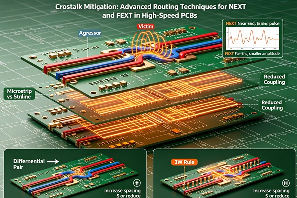
Near-End Crosstalk refers to the interference measured at the end of the victim trace that is closest to the driver of the aggressor trace. NEXT is typically characterized by a backward-traveling wave. Because the induced signal travels back towards the source, NEXT is relatively independent of the coupled length once the coupled length exceeds the spatial extent of the signal’s rising edge. In microstrip and stripline configurations, NEXT is always a factor and often represents the larger magnitude of the two crosstalk types, particularly in dense, short-run routing scenarios.
Far-End Crosstalk (FEXT)
Far-End Crosstalk is measured at the end of the victim trace furthest from the driver of the aggressor trace—in other words, at the receiver end. FEXT is a forward-traveling wave that propagates alongside the aggressor signal. Unlike NEXT, the magnitude of FEXT is directly proportional to the coupled length. A critical distinction lies in the physical layer structure: in a homogenous dielectric environment, such as a perfectly symmetric stripline, capacitive and inductive coupling precisely cancel each other out, resulting in zero FEXT. However, in heterogeneous environments like microstrip layers (where fields exist in both the dielectric substrate and the air), this cancellation does not occur, making FEXT a significant problem for surface-routed high-speed signals.
Advanced Routing Techniques for Crosstalk Mitigation
To achieve robust signal integrity and minimize both NEXT and FEXT, PCB designers must implement a multi-faceted approach utilizing advanced routing techniques.
Managing Trace Spacing and Geometry
The most fundamental rule of crosstalk mitigation is maximizing the physical distance between traces. The strength of electromagnetic coupling is inversely proportional to the square of the distance. Engineers often employ the “3W rule” as a baseline, which dictates that the distance between the centers of two adjacent traces should be at least three times the width of a single trace. For highly sensitive signals or extremely high frequencies, a 5W spacing may be required.
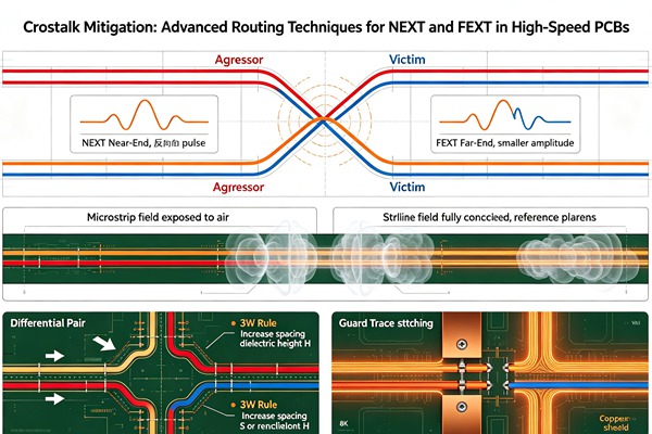
While increasing spacing is effective, it is often constrained by high-density interconnect (HDI) requirements. Therefore, controlling the trace geometry is equally important. Maintaining a consistent characteristic impedance (e.g., 50 ohms single-ended, 100 ohms differential) throughout the routing path minimizes reflections that can exacerbate crosstalk.
Optimizing the Stackup and Reference Planes
The PCB layer stackup plays a crucial role in managing electromagnetic fields. Routing high-speed traces close to a solid, continuous reference plane (either ground or power) is highly effective. The reference plane provides a low-impedance return path and tightly confines the electromagnetic fields between the trace and the plane, significantly reducing the field strength that reaches adjacent traces.
For optimal FEXT mitigation, burying critical high-speed signals in stripline layers (between two solid reference planes) is a best practice. As mentioned, the homogenous dielectric environment of a stripline inherently cancels FEXT. If microstrip routing is unavoidable, minimizing the dielectric thickness between the trace and the reference plane can help tightly couple the signal to its return path, thereby reducing coupling to neighboring traces.
Implementing Orthogonal Routing
When traces must cross each other on adjacent signal layers, they should do so orthogonally (at 90-degree angles). Broadside coupling—where traces run parallel to each other on adjacent layers—must be strictly avoided for high-speed signals. Orthogonal routing minimizes the coupling area to a tiny intersection, effectively eliminating significant crosstalk between those layers. If true orthogonal routing is impossible, crossing at a 45-degree angle is a preferable alternative to parallel routing. Learn more about Conformal Coating: Protecting PCBA from Moisture, Dust, and Corrosive Environments.
Guard Traces and Vias
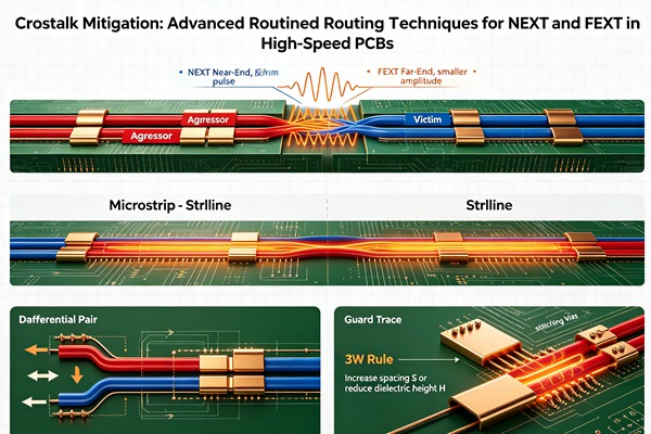
In specific scenarios, introducing guard traces can provide an additional layer of isolation. A guard trace is an electrically grounded trace routed between the aggressor and victim traces. However, guard traces must be implemented with extreme caution. If not properly grounded with frequent vias (stitching vias) along their entire length, they can act as resonant antennas, exacerbating the problem rather than solving it. The distance between stitching vias should be significantly less than one-quarter of the wavelength of the highest frequency component of the signal. Generally, increasing trace spacing is a safer and more predictable approach than relying on guard traces.
Differential Signaling
Differential signaling is a powerful technique for high-speed data transmission, offering inherent immunity to common-mode noise, including crosstalk. A differential pair transmits the signal and its exact inverse simultaneously over two tightly coupled traces. At the receiver, the difference between the two signals is evaluated. Any crosstalk induced on the differential pair will likely affect both traces equally (common-mode noise), and the differential receiver will reject it. To maximize this benefit, the traces within the differential pair must be tightly coupled, perfectly length-matched, and symmetrically routed.
How to Implement a Crosstalk Mitigation Strategy (Step-by-Step Guide)
Follow these engineering rules. Learn more about Embedded Components: Miniaturizing IoT Devices with Embedded PCB Components.
- Perform Pre-Layout Signal Integrity Simulation
Before laying down any copper, utilize advanced signal integrity (SI) simulation software to model critical nets. Define your layer stackup, material properties, and driver/receiver models (IBIS or SPICE). Simulate different trace spacings, lengths, and routing topologies to identify potential crosstalk violations early in the design cycle. Establish design rules based on these simulations.
- Define Critical Nets and Assign Routing Priorities
Identify all high-speed signals, clocks, and sensitive analog lines. Assign them routing priorities. High-speed differential pairs (e.g., PCIe, USB 3.0, SerDes) and fast edge-rate single-ended signals (e.g., DDR memory buses) should be routed first. Segregate these critical nets from noisy aggressive signals like switching power supply nodes or high-current motor drives.
- Establish and Enforce Spacing Rules
Configure your Electronic Design Automation (EDA) tool’s Design Rule Check (DRC) engine to enforce the spacing rules determined during pre-layout simulation. Implement the 3W or 5W rules as baseline constraints for parallel routing of critical nets. Set specific rules for differential pair intra-pair spacing versus inter-pair spacing.
- Optimize Layer Assignment for Stripline Routing
Assign the most critical, highest-speed signals to internal stripline layers. Ensure these layers are sandwiched between solid, continuous ground planes. This step is vital for completely eliminating FEXT and significantly reducing NEXT. Reserve top and bottom microstrip layers for slower signals, power distribution, or signals requiring short, direct connections.
- Minimize Parallel Coupled Lengths
During the routing phase, actively minimize the distance that adjacent traces run parallel to one another. When routing dense buses, such as memory interfaces, look for opportunities to stagger the routing or jog traces to break up long parallel runs. If a long parallel run is unavoidable, increase the spacing between those specific traces beyond the standard DRC rules.
- Implement Orthogonal Crossing on Adjacent Layers
Strictly enforce orthogonal routing for signals that must traverse adjacent signal layers. Never allow high-speed traces to run parallel over top of one another on different layers (broadside coupling). If routing density forces a non-orthogonal crossing, ensure the crossing angle is as steep as possible (e.g., 45 degrees minimum).
- Execute Post-Layout Extraction and Verification
Once the PCB layout is complete, perform a comprehensive post-layout extraction using a 3D field solver or a 2.5D extraction tool. Import the extracted parasitic data (S-parameters) back into your SI simulation environment. Run final simulations to verify that NEXT and FEXT margins are within acceptable limits before releasing the design for manufacturing.
To systematically address NEXT and FEXT in your high-speed PCB designs, follow this structured approach.
The Role of Material Selection in Crosstalk Reduction
While routing geometries and stackup are the primary defense mechanisms against NEXT and FEXT, the dielectric material of the PCB substrate also plays a crucial role. The dielectric constant (Dk) and dissipation factor (Df) directly impact signal propagation speed and attenuation.
Lower Dk materials allow signals to travel faster, which can slightly reduce the effective coupled length for a given physical length. More importantly, in microstrip configurations, materials with tightly controlled and consistent Dk across a wide frequency range help maintain predictable impedance, minimizing reflections that can amplify crosstalk. Learn more about Press-Fit Connectors: PCB Manufacturing Tolerances for Solderless Interconnects.
For ultra-high-speed designs, engineers often transition from standard FR4 materials (which exhibit significant Dk variations and high high-frequency loss) to advanced laminates like Rogers RO4000 series, Megtron 6, or similar low-loss, low-Dk materials. These advanced materials provide a more stable electromagnetic environment, enhancing the effectiveness of the routing techniques discussed above. Learn more about Precision Impedance Control: How to Achieve ±5% Impedance Tolerance in High-Speed PCBs.
Conclusion
Crosstalk mitigation is an intricate balancing act in high-speed PCB design. As edge rates accelerate, the margins for error shrink dramatically. By thoroughly understanding the mechanics of NEXT and FEXT, engineers can apply advanced routing techniques—such as enforcing stringent spacing rules, leveraging stripline topologies, minimizing coupled lengths, and utilizing differential signaling—to safeguard signal integrity. Combined with rigorous pre- and post-layout SI simulations, these practices ensure that complex, high-performance electronic systems operate reliably in demanding real-world environments.
Frequently Asked Questions (FAQ)
The most effective method to eliminate FEXT is to route the critical high-speed signals on internal stripline layers, sandwiched between two continuous ground reference planes. Because a stripline provides a homogenous dielectric environment, the inductive and capacitive coupling coefficients cancel each other out, driving FEXT to zero.
No, the 3W rule applies to the side-by-side spacing of traces on the *same* layer (edge-coupled). For traces on adjacent layers (broadside-coupled), the primary defense is orthogonal routing. If parallel routing on adjacent layers is unavoidable, the vertical distance (dielectric thickness) between them should be maximized, and they should ideally be separated by a reference plane.
No, guard traces can sometimes make crosstalk worse if not implemented correctly. A poorly grounded guard trace can act as a resonant antenna, coupling energy between the aggressor and victim traces. To be effective, a guard trace must be tied to the ground plane with stitching vias spaced closely together (less than 1/10th to 1/4th of the highest frequency wavelength) along its entire length. In many cases, simply increasing the spacing between the aggressor and victim traces is a more reliable solution.
Faster signal rise times (and fall times) contain higher frequency components, which couple more efficiently between adjacent traces. Therefore, a faster edge rate will generate a higher magnitude of NEXT. This is why crosstalk becomes a progressively more severe problem in modern, high-speed digital systems compared to older, slower systems.
While differential signaling provides excellent immunity to common-mode noise (which includes most crosstalk), it does not completely eliminate it. Its effectiveness relies on the crosstalk affecting both traces of the differential pair equally. If the aggressor trace is closer to one trace of the pair than the other, it will induce an unequal (differential) noise voltage, which the receiver cannot entirely reject. Proper routing to ensure tight coupling and symmetry is required to maximize the benefits of differential signaling.