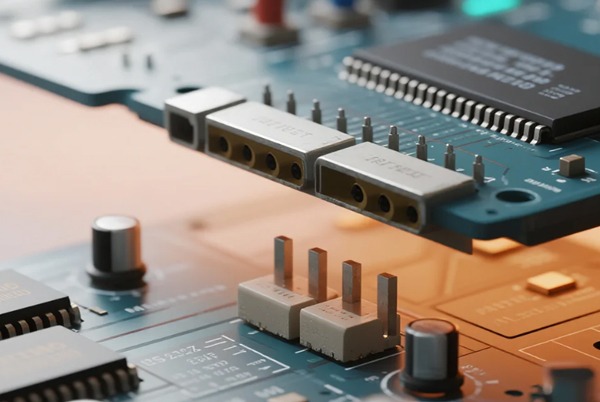
What is a PCB Design? The Essential Guide for Beginners and Engineers
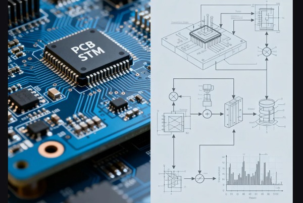
PCB design (Printed Circuit Board design) is a core aspect of electronic engineering that transforms electronic circuits into physical layouts using computer-aided design (CAD) software. Developed since the 1950s, this technology has become indispensable in modern electronics manufacturing. A PCB design is more than just a digital map of electrical connections; it is a complex physical architecture that manages signal timing, heat dissipation, and electromagnetic interference (EMI). A high-quality design ensures that the final product is not only functional but also manufacturable at scale.
At its core, PCB design involves creating a precise “electronic map” that details:
- The exact placement of electronic components
- Connection paths between components (copper traces)
- Conductivity methods between layers (vias)
- Specialized zones (e.g., high-frequency areas, power sections)
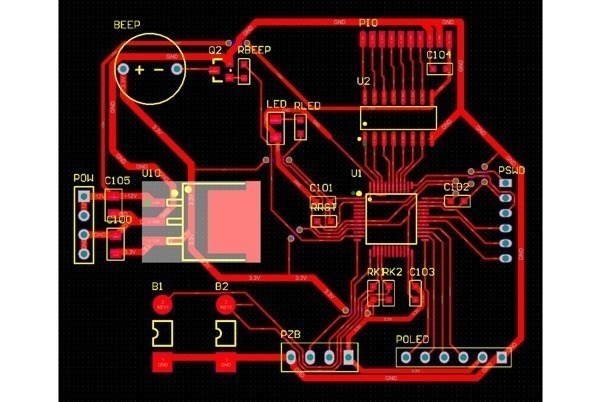
Table of Contents
Key Components of PCB Design
1. Basic Electronic Components
Passive components form the foundation of circuits:
- Resistors: Control current flow, commonly made of carbon or metal film
- Capacitors: Store electrical energy, including ceramic and electrolytic types
- Inductors: Filter high-frequency signals, often used in power circuits
Active components provide “intelligent” functionality:
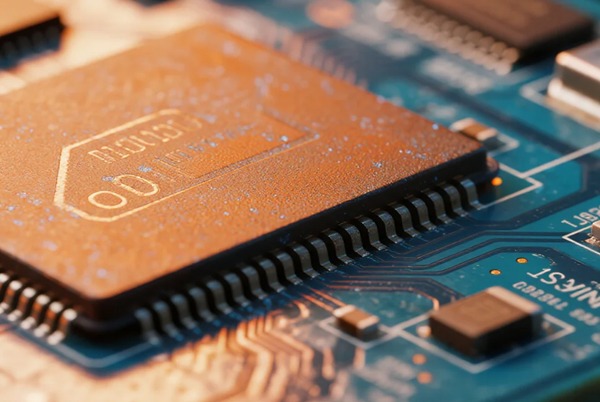
- Integrated Circuits (ICs): Range from simple logic gates to complex microprocessors
- Diodes: Perform rectification, voltage regulation, light emission, etc.
- Transistors: Core elements for signal amplification and switching
2. Connectivity and Interface Systems
- Board-to-board connectors: Ensure reliable connections between PCBs
- User interfaces: Standard ports like USB, HDMI
- Mechanical switches: Enable user interaction
The Complete PCB Design Process
1. Schematic Design Phase
The schematic is the starting point, requiring:
- Accurate component symbol selection
- Clear electrical connections
- Proper net labeling
- Appropriate component parameter settings
Pro Tip: Maintaining a standardized component library significantly improves efficiency.
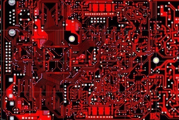
2. PCB Layout Design
Converting schematics into physical layouts involves:
- Mechanical constraints: Mounting holes, enclosure limitations
- Electrical performance: High-speed signal paths, power distribution
- Thermal management: Placement of heat-generating components
- Manufacturing requirements: Minimum trace width, spacing, etc.
3. Design Verification & Optimization
Modern PCB design includes:
- Signal Integrity (SI) analysis
- Power Integrity (PI) analysis
- 3D mechanical assembly checks
- Design for Manufacturability (DFM) validation
Core Considerations in PCB Design
1. Signal Integrity Management
- Impedance matching (critical for high-speed signals)
- Crosstalk reduction (follow the 3W rule)
- Optimized signal return paths
- Proper termination techniques
2. Thermal Design Strategies
- Even distribution of heat-generating components
- Use of high-thermal-conductivity materials
- Thermal via arrays
- Heat sinks or fans, when necessary
3. EMC/EMI Control Techniques
- Layer stackup design
- Shielded enclosures
- Filter circuit placement
- Grounding strategy optimization
PCB Layout Best Practices
1. Component Placement Principles
- Functional modularization
- Consistent signal flow direction
- Isolation of analog/digital sections
- Centralized power system management
2. Routing Techniques
- Prioritize critical signal routing
- Avoid sharp-angle traces
- Length matching for differential pairs
- Widened power traces
3. Grounding System Design
- Star or plane grounding approaches
- Prevent ground loops
- Separate analog/digital grounds
- Multi-point grounding for high-frequency applications
Advanced Design Techniques
1. High-Speed PCB Design Essentials
- Strict impedance control
- Optimized Power Distribution Network (PDN)
- Effective back-drilling techniques
- Consider the dielectric constant stability
2. High-Density Interconnect (HDI) Technology
- Microvia (μVia) implementation
- Any-layer interconnect design
- Embedded component integration
- Fine-line patterning
3. Flexible PCB Design Considerations
- Bend radius control
- Stiffener region design
- Dynamic flexing durability
- Specialized material selection
How to Start a Professional PCB Design Project
- Establish Design Constraints
Define board size, layer count, and material requirements.
- Create a Schematic
Use EDA tools to map out electrical connections.
- Define Layout Rules
Set trace widths and clearances based on voltage and current.
- Execute the Layout
Place components and route traces, ensuring a solid ground plane.
- Generate Fabrication Files
Export Gerber files and a Bill of Materials (BOM) for PCB assembly.
Comprehensive PCB Testing Methods
1. Production Testing Techniques
- In-Circuit Test (ICT): Checks solder quality and component parameters
- Flying Probe Test: Flexible solution for small-batch production
- Automated Optical Inspection (AOI): Detects visual defects
- X-ray Inspection: Examines hidden solder joints (e.g., BGA)
2. Functional Verification Methods
- Burn-in Testing: Extended full-load operation
- Environmental Testing: Extreme temperature, humidity, vibration
- Signal Quality Testing: Eye diagrams, jitter analysis

Industry Trends
- 3D Printed Electronics: Rapid prototyping
- Embedded Components: Higher integration
- AI-Assisted Design: Automated layout/routing
- Sustainable Materials: Eco-friendly PCB solutions
- High-Frequency Materials: 5G/mmWave applications
Engineers can develop high-performance, reliable electronic products that meet increasingly complex market demands by systematically mastering these PCB design principles. Effective PCB design is not just about connectivity—it’s the foundation for successful electronic systems.
PCB Design FAQs
A: Comparison of mainstream tools:
Altium Designer: Professional-grade, full-featured
Cadence OrCAD: Enterprise-level for complex designs
KiCad: Open-source, beginner-friendly
Eagle: Lightweight, suitable for small/medium projects
Recommendation: Consider project complexity, team size, and budget.
A: Structured learning should include:
Fundamentals of electronic circuits
Understanding PCB manufacturing processes
Hands-on CAD software training
Signal integrity basics
Practical project experience
Recommended resources: IPC standards, manufacturer application notes, and professional forums.
A: Key checkpoints:
Trace width/spacing meets factory capabilities
Appropriate drill sizes and aspect ratios
Proper solder mask bridge design
Adequate component spacing for assembly
Sufficient board edge clearance
Pro Tip: Consult PCB manufacturers early for process parameters.
A: PCB design is the holistic process including schematics and logic, while PCB layout specifically refers to the physical placement of components and routing of traces on the board.
A: Industry standards include Altium Designer, KiCad, Cadence Allegro, and Eagle, depending on project complexity and budget.
A: Design for Manufacturing ensures your board can be produced reliably and cost-effectively, preventing expensive redesigns after the prototype stage.
This guide was developed by the Topfast Engineering Team. With 18+ years of experience in PCB Manufacturing, we help engineers turn complex designs into high-performance hardware.


Related Posts