Table of Contents
Introduction: The Imperative for Precision Impedance Control
In the rapidly evolving landscape of high-speed electronics, the margin for error is shrinking at an unprecedented rate. As data rates for architectures such as PCIe Gen 5/Gen 6, 112G PAM4, and 400G/800G Ethernet continue to escalate, maintaining pristine signal integrity (SI) is no longer a best practice—it is an absolute necessity. At these astronomical frequencies, even minor impedance discontinuities can lead to severe signal reflections, increased insertion loss, jitter, and ultimately, a closed eye diagram at the receiver.
Historically, the PCB manufacturing industry standard for controlled impedance has hovered around a ±10% tolerance. For legacy interfaces and lower-speed digital signals, this variance was entirely acceptable. The transceivers could easily compensate for the minor reflections caused by these deviations. However, as rise times plunge into the picosecond domain and voltage swings decrease to minimize power consumption, the traditional ±10% tolerance is proving inadequate. Engineers must now demand precision impedance control, pushing the boundaries of fabrication capabilities to achieve a rigorous ±5% impedance tolerance. Learn more about Conformal Coating: Protecting PCBA from Moisture, Dust, and Corrosive Environments.
Achieving this level of precision is not simply a matter of demanding tighter specifications from a fabrication house. It requires a holistic, synergistic approach that encompasses meticulous material selection, advanced electromagnetic simulation, rigorous stackup design, and an intricate understanding of the manufacturing processes and their inherent limitations. This article delves into the technical intricacies of precision impedance control and outlines a comprehensive methodology for attaining ±5% impedance tolerance in your high-speed printed circuit boards.
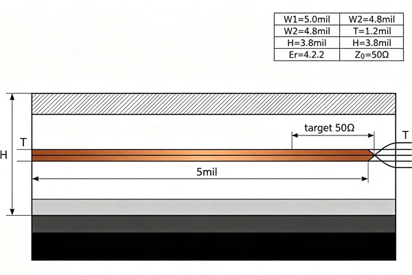
The Physics and Variables Governing Controlled Impedance
To understand how to control impedance tightly, one must first examine the variables that define it. The characteristic impedance ($Z_0$) of a transmission line on a PCB is a functdepends onion of its physical geometry and the electromagnetic properties of the surrounding dielectric materials. Whether dealing with a surface microstrip, an embedded microstrip, or a symmetrical stripline, the fundamental equation for impedance relies on four primary variables:
- Trace Width (W): The width of the copper trace. Impedance is inversely proportional to trace width. Even a deviation of a fraction of a mil (thousandth of an inch) during the etching process can significantly skew the impedance.
- Trace Thickness (T): The height of the copper trace, which is a combination of the base copper weight and any subsequent plating. While its impact is slightly less pronounced than trace width, variations in plating thickness across a panel can jeopardize a ±5% tolerance target.
- Dielectric Thickness (H): The distance between the signal trace and its corresponding reference plane(s). Impedance is directly proportional to dielectric thickness. Controlling the precise thickness of prepreg materials after the lamination press cycle is one of the most challenging aspects of PCB fabrication.
- Dielectric Constant (Dk or Er): The relative permittivity of the PCB substrate. Impedance is inversely proportional to the square root of the Dk. In high-speed designs, the Dk must be highly stable across a wide range of frequencies and temperatures.
The challenge in achieving ±5% impedance tolerance lies in the statistical stack-up of tolerances for each of these variables. If the dielectric thickness runs slightly high while the trace width is etched slightly narrow, the resulting impedance can easily swing beyond the tight ±5% window. Therefore, controlling the final impedance requires controlling the variance of all contributing factors simultaneously. Learn more about PCBA SMT Assembly: Mastering Fine-Pitch BGA and 01005 Components.
Key Drivers for Transitioning to ±5% Impedance Tolerance
Why go through the immense engineering and manufacturing effort required to achieve such strict tolerances? The transition from ±10% to ±5% is driven by several critical electrical requirements in multi-gigabit systems:
- Minimization of Return Loss (Reflections): When a high-speed signal encounters an impedance mismatch, a portion of the signal energy reflects toward the transmitter. This return loss degrades the transmitted signal amplitude and creates inter-symbol interference (ISI). Tighter impedance control minimizes these mismatches at the package-to-board, board-to-connector, and via transitions.
- Preservation of Signal Margins: High-speed serialized data streams rely on intricate equalization techniques (such as DFE and CTLE) to recover the signal. However, these equalizers have finite capabilities. Consuming the SI budget with impedance mismatches leaves less margin for other unavoidable losses, such as conductor skin effect and dielectric absorption.
- Channel Resonance Mitigation: In complex topologies with multiple discontinuities (e.g., via stubs, connector interfaces), variations in trace impedance can shift the resonant frequencies of the channel. A ±5% tolerance ensures that the channel behavior aligns perfectly with pre-layout simulations, preventing unexpected resonant nulls within the operating frequency band.
- Lower Voltage Swings: Modern silicon operates at heavily reduced core and I/O voltages. With smaller peak-to-peak voltage swings, any noise introduced by reflections constitutes a much larger percentage of the total signal amplitude, making tight impedance control vital for maintaining an acceptable Signal-to-Noise Ratio (SNR).
How to Achieve ±5% Impedance Tolerance (Step-by-Step Guide)
Follow these engineering rules.
- Select Ultra-Stable High-Speed Laminates
The foundation of precision impedance is the substrate material. Standard FR-4 laminates exhibit significant variations in Dielectric Constant (Dk) and Dissipation Factor (Df) across different frequencies and resin contents. To achieve ±5% tolerance, you must select high-performance, low-loss materials engineered specifically for high-speed digital applications (e.g., Megtron 6/7, Rogers RO4000 series, or advanced Isola products). These materials offer a flat Dk response over a broad frequency spectrum and boast excellent dimensional stability, ensuring that the dielectric thickness remains predictable during the lamination cycle.
- Perform Advanced Pre-Layout Simulation and Modeling
Before routing a single trace, utilize advanced 2D and 3D electromagnetic field solvers (such as Ansys HFSS, Altair PollEx, or Polar Speedstack) to model the transmission lines accurately. Standard impedance calculators often lack the fidelity required for ±5% tolerances because they may ignore secondary effects like the trapezoidal shape of etched traces, solder mask loading, or copper surface roughness. Pre-layout simulation allows you to sweep variables and establish a nominal design that sits squarely in the center of the manufacturing window, providing the maximum possible buffer for fabrication variances.
- Implement Strict Stackup Design and Glass Weave Selection
The PCB stackup dictates the dielectric thickness (H), which is the most sensitive variable in the impedance equation. Work intimately with your fabricator to construct a stackup using specific prepreg and core materials that they have thoroughly characterized. Furthermore, address the “glass weave effect.” Standard PCB substrates consist of woven glass bundles impregnated with resin. Because glass and resin have different Dk values, a trace routed directly over a glass bundle will experience a different impedance than a trace routed over the resin-rich gaps. For precision control, specify mechanically spread glass weaves (such as 1067, 1086, or 1078 styles) or route high-speed signals at a slight angle (e.g., 10 degrees) to the weave to average out the Dk variations.
- Optimize Trace Geometry and Routing Topologies
Design your trace geometries to minimize the impact of manufacturing tolerances. For example, opting for slightly wider traces and thicker dielectrics can reduce the percentage impact of a standard 0.5 mil etching variation compared to using ultra-fine traces. Maintain consistent routing topologies. Avoid acute angles and ensure continuous reference planes. When transitioning between layers, design impedance-matched vias by optimizing the anti-pad dimensions and removing unused internal via pads (non-functional pads) to minimize parasitic capacitance, which drastically lowers the localized impedance.
- Partner with an Advanced PCB Manufacturer for Process Control
Achieving ±5% impedance is ultimately a manufacturing feat. You must partner with a Tier-1 PCB fabricator that employs advanced statistical process control (SPC). The manufacturer must utilize precise laser direct imaging (LDI) for exact trace width definition, employ specialized etch chemistry with real-time concentration monitoring to control the trapezoidal etch factor, and utilize specialized vacuum presses that maintain uniform pressure and temperature profiles to guarantee consistent prepreg thickness. They should also possess advanced Time Domain Reflectometry (TDR) testing equipment to verify the final impedance of the fabricated coupons.
Attaining precision impedance control is an iterative process that requires tight collaboration between the hardware design team, the signal integrity engineers, and the PCB manufacturer. Follow these essential steps to ensure success.
Overcoming Manufacturing Variations and Tolerances
Even with the best design practices, manufacturing is not perfect. The key to hitting a ±5% tolerance target is compensating for known manufacturing behaviors during the design and tooling phases. Learn more about Hard Gold Plating: Edge Connectors and Switch Contacts Design for Extreme Wear Resistance.
Experienced fabricators apply an “etch compensation” factor to the original gerber data. Because the chemical etching process naturally removes slightly more copper at the top of the trace than at the base, traces become trapezoidal rather than perfectly rectangular. If a designer requires a 4.0 mil trace, the fabricator might image a 4.5 mil trace on the photoresist, anticipating that the etch process will reduce it to the target dimensions.
Furthermore, copper plating thickness can vary across the surface of a panel due to uneven current density during the electroplating process. Advanced fabricators combat this by adding “thieving” patterns—non-functional copper structures placed in empty areas of the board—to balance the localized current density and ensure uniform plating thickness, thereby preventing impedance variations across different regions of the PCB. Learn more about Via-in-Pad Plated Over (VIPPO): Design Guidelines for Fine-Pitch BGA Breakout.
Frequently Asked Questions (FAQ)
Standard ±10% tolerance is often insufficient for modern high-speed protocols (like PCIe Gen 5/6 or 112G Ethernet) because the dramatically faster rise times and smaller voltage swings leave very little margin for error. Impedance mismatches of 10% can cause significant signal reflections, leading to increased jitter, severe inter-symbol interference (ISI), and eye diagram closure, which ultimately results in data transmission errors.
To achieve a ±5% tolerance, engineers should avoid standard FR-4 and instead opt for high-speed, low-loss laminates. Materials such as Panasonic Megtron 6 or 7, Isola Tachyon, or Rogers RO4000 series are highly recommended. These laminates offer exceptionally stable Dielectric Constants (Dk) across wide frequency ranges and varying environmental conditions, alongside superior dimensional stability during the lamination process.
The glass weave effect occurs because the fiberglass bundles (high Dk) and the surrounding epoxy resin (low Dk) in a PCB substrate have different dielectric properties. If a differential pair or single-ended trace runs parallel to these bundles, it can experience micro-variations in impedance and phase skew. To maintain ±5% precision, it is critical to use spread-glass styles or route traces at an angle to the weave to homogenize the effective Dk the signal “sees.”
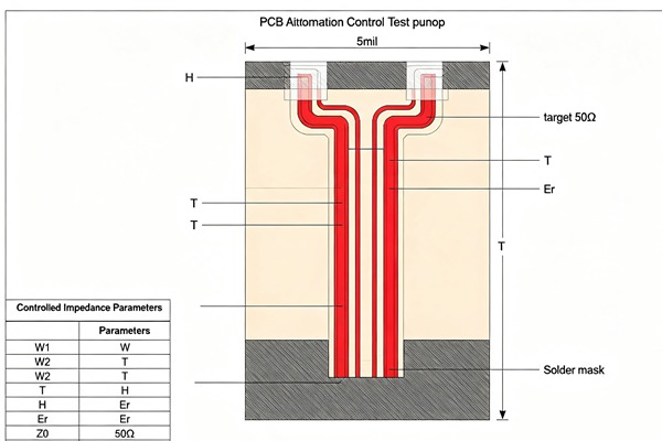
Manufacturers verify impedance using Time Domain Reflectometry (TDR) equipment. Because it is often impractical to measure the actual traces on the production board due to access limitations and via effects, fabricators typically place “impedance coupons” on the edges of the manufacturing panel. These coupons contain straight test traces designed to exactly mimic the trace widths, clearances, and stackup of the actual PCB. The TDR sends a fast step pulse into the coupon and measures the reflected energy to precisely calculate the characteristic impedance.