The harsh environment of aerospace applications presents unparalleled challenges for electronics. From the unforgiving vacuum of Low Earth Orbit (LEO) to the high-friction descent of reentry vehicles, aerospace printed circuit boards (PCBs) must endure extreme environmental stressors. Among the most destructive of these stressors is extreme thermal cycling—the rapid and repeated fluctuation of temperatures across wide extremes, often ranging from -150°C in the shadow of the Earth to well over +150°C under direct solar radiation.
In commercial electronics, standard FR-4 laminates and typical lead-free solders are generally sufficient. However, deploying such materials in a satellite, deep-space probe, or high-altitude military aircraft is a recipe for catastrophic failure. In these mission-critical applications, maintenance is impossible, and the cost of failure is measured not just in millions of dollars, but potentially in the loss of critical mission objectives or human life. Therefore, mastering the intricacies of extreme thermal cycling, executing rigorous reliability testing, and specifying the correct materials are paramount tasks for aerospace PCB engineers.
Table of Contents
The Physics of Thermal Cycling in Printed Circuit Boards
To understand why thermal cycling is so destructive, one must first examine the physics of thermal expansion. All materials expand when heated and contract when cooled, a property quantified by the Coefficient of Thermal Expansion (CTE). A printed circuit board is a complex, heterogeneous composite made of dielectric resins, woven glass reinforcement, copper traces, plated vias, and various component packages.
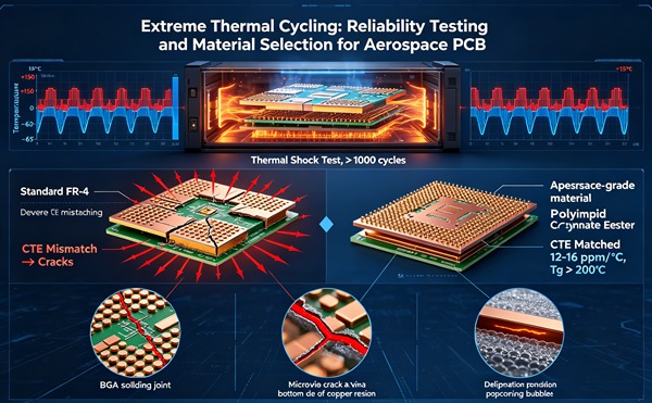
Because these materials possess vastly different CTE values, thermal cycling induces severe mechanical stress. For instance, the copper forming a Plated Through-Hole (PTH) expands at a rate of approximately 17 ppm/°C. The surrounding dielectric material in the Z-axis (thickness) often expands at a rate of 40 to 70 ppm/°C below the Glass Transition Temperature (Tg), and can skyrocket to over 250 ppm/°C above the Tg. Learn more about PCBA SMT Assembly: Mastering Fine-Pitch BGA and 01005 Components.
During a thermal excursion, the resin expands significantly more than the copper barrel of the via. This CTE mismatch places the copper under immense tensile stress during the heating phase and compressive stress during the cooling phase. Over hundreds or thousands of cycles, this cyclic loading leads to metal fatigue, work hardening, and ultimately, mechanical fracture.
Common Failure Mechanisms Induced by Extreme Thermal Cycling
When aerospace PCBs are subjected to extreme thermal cycling, several distinct failure mechanisms can manifest, each capable of rendering the electronic assembly non-functional. Learn more about Precision Impedance Control: How to Achieve ±5% Impedance Tolerance in High-Speed PCBs.
Plated Through-Hole (PTH) Fatigue and Barrel Cracking
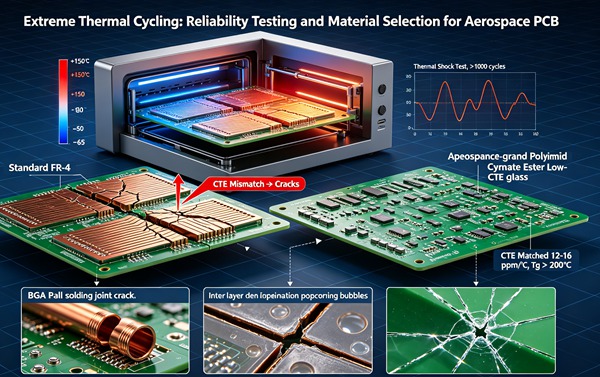
As described above, Z-axis expansion is the primary enemy of the PTH. The stress concentrates at the midpoint of the barrel or at the interface between the barrel and the internal copper layers (the inner layer interconnect). Microcracks begin to form in the copper plating, propagating with each subsequent thermal cycle until a complete open circuit occurs. Learn more about Stacked vs. Staggered Microvias: Design Rules and Reliability in High-Density Interconnect (HDI) PCBs.
Solder Joint Fatigue
Surface-mount technology (SMT) components are soldered directly to the board’s surface. If the CTE of a component package (such as a large ceramic BGA) differs significantly from the CTE of the PCB substrate (X-Y axis), sheer stress is exerted on the solder joints during thermal cycling. Over time, the solder undergoes creep and fatigue, leading to crack initiation and propagation through the bulk solder or along the intermetallic compound (IMC) layer.
Pad Cratering and Delamination
In instances where the solder joint is stronger than the underlying dielectric material, the stress from thermal cycling can cause the pad to be ripped entirely from the substrate, taking a crater of resin with it. Alternatively, repeated thermal shock can cause the adhesive bonds between the different layers of the PCB to fail, resulting in delamination or blistering.
Conductive Anodic Filament (CAF) Growth
While thermal cycling itself does not directly cause CAF, the microcracking and interfacial breakdown caused by thermomechanical stress create pathways for moisture and electrolyte ingress. Under an applied voltage bias, this can lead to the electrochemical migration of copper, forming a conductive filament that causes a catastrophic short circuit between adjacent traces or vias.
Material Selection Strategies for Aerospace PCBs
Mitigating the effects of extreme thermal cycling begins with intelligent material selection. Standard materials are woefully inadequate; aerospace applications demand high-performance, specialized substrates.
High Tg and Low Z-Axis CTE Laminates
The Glass Transition Temperature (Tg) is the point at which a resin changes from a rigid, glassy state to a softer, rubbery state, accompanied by a massive increase in CTE. For aerospace PCBs, selecting a material with a high Tg (typically >170°C, and often >200°C) is essential to ensure the operating temperature rarely, if ever, exceeds the Tg. Furthermore, specialized resin formulations incorporating fillers can suppress the Z-axis CTE, drastically reducing the strain on plated through-holes.
Polyimide Resins
Polyimide is a staple in aerospace PCB manufacturing. It boasts an incredibly high Tg (often exceeding 250°C), exceptional thermal stability, and robust resistance to extreme temperature fluctuations. While it is more difficult to process and more expensive than traditional epoxy resins, its reliability in harsh environments makes it the material of choice for high-reliability military and space applications.
PTFE (Teflon) and Advanced Thermosets
For high-frequency RF applications common in aerospace communication systems, PTFE-based laminates are frequently utilized. While pure PTFE has a very high CTE, commercial RF materials blend PTFE with ceramic fillers and woven glass to create a composite with tailored dielectric properties and manageable thermomechanical stability.
Copper Foil Considerations
The ductility of the copper foil is critical. Electrodeposited (ED) copper is standard, but for applications involving extreme thermal stress or flex-rigid sections, Rolled Annealed (RA) copper offers superior ductility and fatigue resistance. Additionally, specifying thicker minimum copper plating in the via barrels (e.g., 1 mil or greater, as per IPC-6012 Class 3/A standards) provides more mechanical robustness against Z-axis expansion. Learn more about M-SAP Technology: Achieving Sub-25 Micron Line/Space for Next-Generation Electronics.
How to Conduct Reliability Testing for Aerospace PCBs (Step-by-Step Guide)
Follow these engineering rules.
- Define the Mission Profile and Environmental Parameters
Before testing begins, engineers must meticulously define the expected thermal environment. This includes the minimum and maximum temperatures, the dwell time at extreme temperatures, the rate of temperature change (ramp rate), and the total number of cycles expected over the mission’s operational lifespan.
- Select the Appropriate Testing Standards
Utilize established industry standards to govern the testing protocol. For aerospace, MIL-PRF-31032, IPC-6012 (Class 3 and 3/A for space applications), and specific NASA or ESA standard requirements often dictate the test conditions, acceptance criteria, and quality conformance inspections.
- Design the Test Vehicles and Coupons
Do not test the final production board initially; instead, design specialized Interconnect Stress Test (IST) coupons or specific test vehicles. These coupons should feature daisy-chained via networks, representative component footprints, and trace routing that mirrors the most challenging aspects of the actual PCB design.
- Execute the Thermal Cycling Protocol
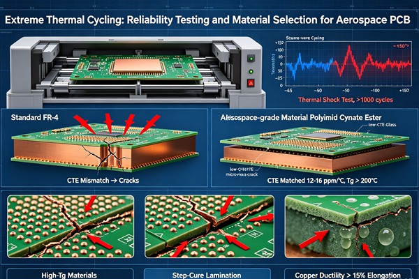
Place the test vehicles in a highly controlled environmental chamber capable of rapid thermal transitions. A typical aerospace thermal cycle might involve ramping from -55°C to +125°C, or even -65°C to +150°C. Ensure the thermal mass of the chamber is sufficient to guarantee the boards themselves reach the target temperatures and dwell there for the required duration to achieve thermal equilibrium.
- Perform In-Situ Electrical Monitoring
Continuous, in-situ resistance monitoring is vital. Unlike post-test probing, continuously measuring the resistance of the daisy-chained networks during the thermal cycling allows engineers to detect intermittent opens. An increase in resistance (typically 10% above the baseline) indicates the onset of microcracking and constitutes a failure, even if the connection restores itself at room temperature.
- Conduct Post-Test Destructive and Non-Destructive Analysis
Once the test vehicles have failed or completed the required number of cycles, conduct thorough analysis. Begin with non-destructive techniques such as Scanning Acoustic Microscopy (SAM) or 3D X-ray CT to locate delamination and gross structural anomalies. Follow this with destructive microsectioning (cross-sectioning) to visually inspect the vias, inner layer interconnects, and solder joints under high magnification.
- Analyze Data and Refine the Design
Utilize the failure data, such as Weibull distributions, to calculate the Mean Time to Failure (MTTF) and compare it against the mission requirements. If the design fails prematurely, iterate on the material selection, via geometries, or board stackup to enhance thermomechanical robustness.
To guarantee that a PCB assembly will survive its intended environment, it must undergo rigorous accelerated life testing. Below is the methodology for validating aerospace PCB reliability.
Advanced Mitigation Strategies
Beyond substrate selection, mechanical mitigation strategies play a vital role. Conformal coatings (such as Parylene) and potting compounds can encapsulate the board, protecting it from moisture and outgassing, though their own CTE must be carefully matched to avoid inducing additional stress.
Furthermore, strategic component placement is critical. Placing large, rigid components near the center of the board rather than the edges minimizes the bending moments induced by thermal warping. Lastly, minimizing the use of microvias stacked on top of one another (stacked vias) in favor of staggered microvias can significantly reduce stress concentrations in high-density interconnect (HDI) designs.
Frequently Asked Questions (FAQ)
Typical aerospace thermal cycling tests range from -55°C to +125°C for military and aviation applications. However, space applications (satellites and probes) often require testing from -65°C to +150°C, and in severe cases like lunar or deep-space missions, the lower limit can drop below -100°C.
Polyimide is preferred because it possesses a significantly higher Glass Transition Temperature (Tg), superior thermal stability, and excellent resistance to radiation and outgassing in a vacuum. Unlike FR4, which can degrade or experience massive thermal expansion at extreme temperatures, polyimide maintains its structural integrity and mechanical properties in harsh environments.
CTE mismatch occurs when materials bonded together expand and contract at different rates during temperature changes. In a PCB, the resin expands significantly more in the Z-axis than the copper vias. This creates severe cyclic tensile and compressive stresses, eventually causing metal fatigue and cracking in the copper structures or solder joints.
IPC-6012 Class 3/A is an advanced standard specifically tailored for space and military avionics. It imposes far more stringent requirements than standard Class 3, including thicker minimum copper plating in vias, tighter annular ring requirements, and more rigorous inspection criteria, ensuring the highest level of reliability for critical missions.
No. While Finite Element Analysis (FEA) and thermal simulation software are invaluable tools for predicting stress hotspots and optimizing designs early in the development cycle, they rely on idealized material models. Physical thermal cycling remains a mandatory validation step to account for manufacturing variations, complex material interactions, and unpredictable real-world failure modes.