As electronic devices continue their relentless march towards miniaturization and higher performance, printed circuit board (PCB) layouts have become increasingly complex. High-Density Interconnect (HDI) technology is the bedrock of modern electronics, enabling the routing of fine-pitch components like Ball Grid Arrays (BGAs) and highly integrated system-on-chips (SoCs). At the heart of HDI PCB fabrication are microvias—laser-drilled holes typically 6 mils (150 micrometers) or less in diameter that connect adjacent or closely spaced layers. Learn more about M-SAP Technology: Achieving Sub-25 Micron Line/Space for Next-Generation Electronics.
When routing multi-layer HDI structures, engineers must traverse multiple dielectric layers to reach the inner routing channels. This necessitates the use of multiple microvias in succession. The structural arrangement of these successive microvias falls into two primary categories: stacked microvias and staggered microvias. Learn more about Ceramic PCBs: Alumina vs. Aluminum Nitride (AlN) Ceramic PCBs for Extreme Heat.
Choosing between a stacked and a staggered microvia architecture is not merely a matter of routing convenience; it is a critical engineering decision that dictates the manufacturability, signal integrity, and long-term thermomechanical reliability of the final product. This article delves into the technical disparities between stacked and staggered microvias, outlining the design rules, reliability concerns, and manufacturing considerations essential for B2B engineering teams developing mission-critical hardware. Learn more about Sequential Lamination: Mastering the Manufacturing Process for Any-Layer HDI Boards.
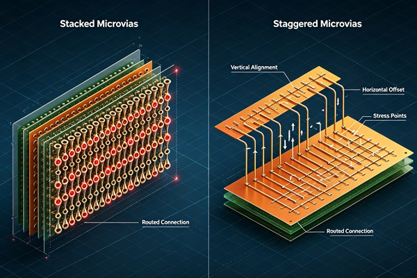
Table of Contents
Understanding Microvia Architectures in HDI
To appreciate the design trade-offs, it is necessary to first define the physical configurations of both via types in the context of sequential lamination, the process by which HDI PCBs are built layer by layer. Learn more about Embedded Components: Miniaturizing IoT Devices with Embedded PCB Components.
Stacked Microvias
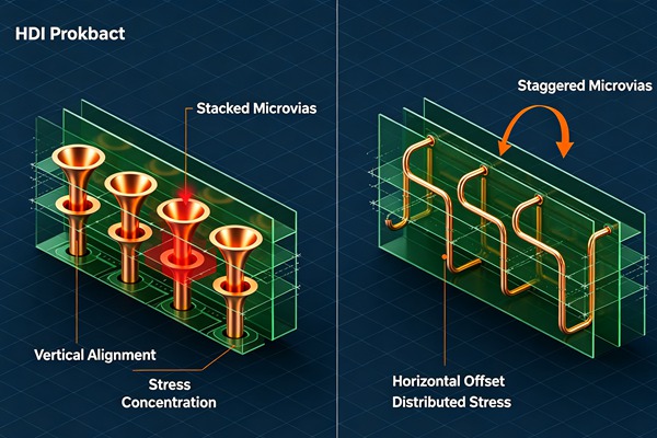
A stacked microvia structure occurs when multiple laser-drilled microvias are aligned exactly on top of one another along the Z-axis, connecting three or more layers in a straight vertical path. For example, a microvia connecting layer 1 to layer 2 is placed directly above a microvia connecting layer 2 to layer 3.
The primary advantage of stacked microvias is space efficiency. Because they occupy the exact same X-Y coordinate across multiple layers, they consume the absolute minimum amount of board real estate. This makes them highly attractive for routing out of incredibly dense components, such as 0.4mm pitch BGAs, where escape routing channels are severely constrained. Furthermore, from a signal integrity perspective, a perfectly vertical, stacked structure minimizes capacitive stubs and provides a direct, low-inductance path for high-speed signals.
However, to create a stacked structure, the underlying microvia must be completely filled with electroplated copper to provide a flat, solid planar surface for the subsequent via to be drilled and plated onto. This solid copper pillar design is where the reliability challenges originate.
Staggered Microvias
In a staggered microvia architecture, the microvias connecting sequential layers are physically offset from one another in the X-Y plane. For instance, the microvia from layer 1 to 2 will land on a capture pad, and the microvia from layer 2 to 3 will originate from a different location on that same layer 2 pad (or a connected trace), dropping down to the next layer.
This configuration requires slightly more board space because the capture pads for the sequential vias do not perfectly overlap. However, this geometric offset inherently alters the stress distribution within the PCB during thermal cycling. Because the vias are not in a single vertical column, the underlying via does not necessarily need to be completely solid copper-filled (though it often is for other process reasons), and the stress vectors are distributed laterally across the dielectric and copper interfaces rather than being concentrated at a single, multi-layer Z-axis point.
Thermomechanical Reliability: The Core Differentiator
The defining difference between stacked and staggered microvias lies in their thermomechanical reliability, particularly during lead-free solder reflow profiles (which can exceed 250°C) and long-term environmental thermal cycling.
PCBs are composite structures consisting of copper and dielectric materials (like FR4, polyimide, or advanced high-speed laminates). These materials possess vastly different Coefficients of Thermal Expansion (CTE). Copper expands at approximately 16-18 ppm/°C, while standard FR4 dielectric expands at 50-70 ppm/°C in the Z-axis (above the glass transition temperature, Tg, this expands even more aggressively).
When an HDI board undergoes thermal excursion, the dielectric material expands significantly more in the Z-axis than the copper vias. This creates severe Z-axis strain.
In stacked microvias, this strain is concentrated entirely along the single vertical axis of the copper pillar. The weakest link in this structure is typically the interface between the target pad and the bottom of the plated via, often referred to as the target pad separation interface. If the stress exceeds the tensile strength of this electroplated/electroless copper interface, a micro-crack will form, leading to an open circuit. The IPC (Association Connecting Electronics Industries) has issued numerous warnings and addendums, notably in IPC-6012E, highlighting the inherent reliability risks of stacked microvias, especially when stacking three or more layers (e.g., 3-N-3 HDI structures).
Conversely, staggered microvias decouple this Z-axis stress. Because the vias are offset, the Z-axis expansion of the dielectric material cannot act upon a single, continuous copper pillar. The stress is dissipated through the intermediate capture pads and the surrounding dielectric. Empirical data and highly accelerated thermal shock (HATS) testing consistently demonstrate that staggered microvia configurations survive significantly more thermal cycles before failure compared to their stacked counterparts. For high-reliability applications—such as aerospace, automotive ADAS (Advanced Driver Assistance Systems), and medical devices—staggered microvias are overwhelmingly preferred.
Design Rules for Stacked Microvias
If routing density dictates the use of stacked microvias, stringent design rules must be enforced to mitigate reliability risks.
- Via Filling: Stacked vias absolutely must utilize bottom-up copper plating to ensure a void-free, solid copper structure. Any voids or dimples in the underlying via will cause plating defects and stress concentrations in the subsequent stacked via.
- Aspect Ratio: The aspect ratio (dielectric thickness to drilled hole diameter) of each individual microvia should ideally be kept below 0.8:1, and preferably closer to 0.5:1. Shallower vias are easier to plate reliably and exhibit lower stress concentrations.
- Limit the Stack: Avoid stacking more than two microvias (e.g., L1-L2, L2-L3). Stacking three or more microvias increases the probability of target pad separation exponentially.
- Pad and Annular Ring Sizing: Maintain robust capture and target pads. While HDI implies small pads, shrinking the target pad too aggressively reduces the surface area available for the metallurgical bond, weakening the via structure.
- Material Selection: Utilize high-Tg, low-CTE dielectric materials. Reducing the volumetric expansion of the surrounding resin system is the most effective way to reduce the applied stress on the copper via structure.
Design Rules for Staggered Microvias
Designing with staggered microvias involves managing the offset geometry to ensure manufacturability and electrical performance.
- Minimum Stagger Offset: The critical dimension is the distance between the center point of the upper via and the center point of the lower via. A standard industry rule is that the offset should be at least equal to the microvia diameter plus a safety margin to prevent breakout.
- Tangent vs. Separated Stagger: Vias can be staggered such that their drilled holes are tangent (touching at the edge) or fully separated. Fully separated vias (where the drill edges do not overlap in the Z-axis) are generally preferred for reliability, as tangent vias can still share localized stress concentrations.
- Routing Channel Impact: Designers must account for the larger composite footprint of a staggered structure. This requires careful fan-out planning under dense BGAs to ensure the staggered pads do not block adjacent routing channels on the inner layers.
- Layer Pair Pairing: Sequential lamination requires specific layer pairs to be processed together. When designing staggered vias, ensure that the stagger pattern aligns with the fabricator’s planned lamination cycles.
How to Choose the Right Microvia Structure (Step-by-Step Guide)
Follow these engineering rules.
- Evaluate Routing Density Requirements
Begin by analyzing the pin pitch and I/O count of your most complex components. Determine if the ultra-high density of stacked microvias is strictly necessary to escape the component footprint. If the routing can be accomplished using staggered vias without adding unnecessary signal layers, staggered should be the default choice.
- Analyze the Operating Environment
Assess the lifecycle thermal cycling requirements, extreme temperature operating ranges, and expected lifespan of the product. Applications exposed to harsh environments, automotive under-hood conditions, or demanding aerospace profiles must prioritize the thermomechanical robustness of staggered microvias over the space savings of stacked architectures.
- Consult with Your PCB Manufacturer
Before finalizing a stackup, engage with your chosen PCB fabricator. Verify their specific capabilities regarding laser drilling accuracy, sequential lamination cycles, and their process controls for void-free copper filling. A fabricator’s yield history can heavily influence the decision between stacked and staggered designs.
- Perform Signal Integrity Analysis
Simulate the high-speed signal paths, particularly those exceeding 10 Gbps, to ensure that the chosen via structure does not introduce unacceptable impedance discontinuities. While stacked vias offer a slightly shorter electrical path, staggered vias can often be optimized with careful pad design and reference plane management to meet stringent signal integrity targets.
- Finalize the Stackup and Route
Implement the design utilizing staggered microvias as the default methodology for maximum reliability. Employ stacked microvias exclusively in the specific, localized areas where routing constraints absolutely dictate their use, thereby minimizing the overall risk profile of the PCB assembly.
Selecting between stacked and staggered configurations requires a systematic approach, balancing electrical needs with manufacturability and long-term reliability.
Manufacturing Challenges and Cost Implications
The manufacturing processes for HDI boards are inherently more complex and expensive than standard multilayer PCBs due to sequential lamination. Every sub-assembly cycle requires inner-layer imaging, etching, lamination, laser drilling, desmear, and plating.
Stacked microvias drive cost up primarily due to the specialized plating chemistry and extended time required for void-free copper filling. Bottom-up plating is a slower process than standard conformal plating. Furthermore, if the top via in a stack is slightly misregistered over the bottom via, the laser drill can damage the edge of the underlying copper pillar, leading to immediate plating failures or latent reliability defects.
Staggered microvias alleviate the strict requirement for perfectly flat, solid copper filling (though it is still standard practice in many high-end fabs). The relaxed Z-axis registration tolerances improve manufacturing yields. Because they are less prone to catastrophic failure during the thermal stress of assembly (reflow), the overall delivered yield of the populated board is often higher, offsetting the minor footprint penalty.
In conclusion, while stacked microvias offer the ultimate solution for extreme miniaturization, they demand rigorous design adherence, premium materials, and elite fabrication capabilities to survive thermal stress. Staggered microvias present a more robust, forgiving architecture that should be the preferred choice for B2B engineering designs where long-term reliability is paramount.
Frequently Asked Questions (FAQ)
The primary cause of failure in stacked microvias is thermomechanical fatigue induced by the Coefficient of Thermal Expansion (CTE) mismatch between the copper plating and the dielectric material during thermal cycling, leading to target pad separation or barrel cracking.
Yes, it is common practice to mix both architectures on a single High-Density Interconnect (HDI) board. Designers often use staggered microvias for the majority of the routing to maximize reliability and reserve stacked microvias exclusively for areas under fine-pitch components where routing space is absolutely restricted.
Absolutely. Selecting a dielectric material with a high glass transition temperature (Tg) and a low Coefficient of Thermal Expansion (CTE) significantly reduces the stress exerted on the microvia structures during thermal excursions, thereby improving the overall reliability of the PCB.
Not always, but they often yield better. While both require sequential lamination, staggered microvias are less sensitive to microscopic registration errors and do not strictly mandate the expensive, time-consuming void-free bottom-up copper plating required for stacked vias. This generally translates to higher manufacturing yields and lower overall fallout costs.