Table of Contents
Introduction to Zero-Defect PCB Assembly
In the highly competitive and precision-driven landscape of modern electronics manufacturing, achieving zero-defect Printed Circuit Board Assembly (PCBA) is no longer merely an aspirational goal—it is a mandatory operational requirement. As electronic devices become exponentially smaller, denser, and fundamentally mission-critical in sectors such as aerospace avionics, implantable medical devices, automotive (particularly advanced driver-assistance systems and electric vehicles), and 5G telecommunications infrastructure, the cost of field failure has escalated dramatically. A single undetected solder bridge, a misaligned passive component, or a microscopic void in a Ball Grid Array (BGA) can lead to catastrophic system-level failures, exorbitant warranty recalls, and severe brand damage.
To effectively mitigate these risks and ensure absolute reliability across the entire production run, electronics contract manufacturers and OEMs rely heavily on advanced, automated inspection technologies. Chief among these diagnostic tools are Automated Optical Inspection (AOI) and 3D X-Ray Inspection (widely known as Automated X-Ray Inspection, or AXI). While each inspection technology is highly capable in its own distinct operational domain, their combined, strategic application forms the absolute bedrock of a comprehensive zero-defect manufacturing strategy. This article delves deeply into the technical mechanics, defect detection capabilities, and synergistic implementation of AOI and 3D X-Ray systems within modern Surface Mount Technology (SMT) production lines.
Automated Optical Inspection (AOI): The First Line of Defense
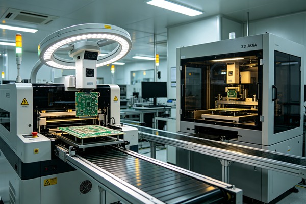
Automated Optical Inspection (AOI) has evolved significantly from its early, logic-limited 2D iterations. Today, true 3D AOI stands as the industry standard, utilizing ultra-high-resolution industrial cameras, sophisticated multi-angle directional lighting arrays, and computationally intensive algorithms to visually inspect PCBs at various critical stages of the assembly process. Learn more about Press-Fit Connectors: PCB Manufacturing Tolerances for Solderless Interconnects.
The Mechanics of 3D AOI
Modern 3D AOI systems primarily employ fringe projection technology, phase shift profilometry, or moiré interferometry to capture highly accurate, granular topographic data of the entire PCBA surface. In practice, multiple integrated projectors cast precise, structured light patterns onto the board. Concurrently, high-speed cameras capture the resulting microscopic deformations in this light pattern as it drapes over components and solder joints. By rigorously mathematically analyzing these phase shifts and deformations, the system software constructs a precise, mathematically accurate 3D model of the board. This allows for true volumetric measurements of component bodies and the specific geometry of solder fillets. Learn more about Crosstalk Mitigation: Advanced Routing Techniques to Minimize NEXT and FEXT in High-Speed PCBs.
This transition to 3D profiling is mission-critical. Traditional 2D AOI heavily relied on contrast and edge detection, which notoriously struggled with shadows from taller adjacent components, subtle board warpage, and unpredictable component color or reflectivity variations from different suppliers. This often led to unacceptably high false-call (pseudo-defect) rates, forcing human operators to waste time verifying perfectly good boards. 3D AOI decisively overcomes these inherent limitations by relying on immutable volumetric spatial data rather than easily skewed 2D pixel contrast.
Key Defect Detections by AOI
AOI is strategically deployed at multiple distinct intervention points across the SMT line: post-solder paste printing (SPI – Solder Paste Inspection, technically a dedicated subset of optical inspection), pre-reflow (post-placement), and post-reflow. Post-reflow AOI is particularly critical for definitively identifying a wide array of surface-level anomalies:
- Component Presence and Absolute Alignment: Verifying that the correct component is populated, perfectly centered on its designated pads, and rotationally accurate (X, Y, and Theta coordinates).
- Polarity and Laser Markings: Utilizing advanced Optical Character Recognition and Verification (OCR/OCV) to read component markings and ensure polarized components—such as electrolytic capacitors, diodes, and ICs—are oriented precisely as defined by the CAD data.
- Tombstoning and Billboarding: Reliably detecting passive components (like 0402 or 0201 resistors) that have unevenly wetted and subsequently lifted off one pad during the thermal reflow process, standing vertically or on their side.
- Solder Bridging and Shorts: Identifying unwanted solder web connections between adjacent fine-pitch pins on components like QFPs (Quad Flat Packages) or SOICs.
- Missing, Insufficient, or Excess Solder: Analyzing the complete 3D solder fillet volume and wetting angle to ensure adequate intermetallic bonding and mechanical strength, strictly adhering to IPC-A-610 standards.
Despite its exceptional speed and analytical prowess, AOI has one fundamental physical limitation: it strictly requires an unobstructed direct line of sight. It fundamentally cannot inspect what it cannot optically see.
The Role of 3D X-Ray Inspection (AXI)
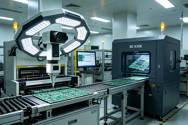
As advanced packaging technology aggressively advances toward higher I/O densities and miniaturization, components like BGAs (Ball Grid Arrays), CSPs (Chip Scale Packages), Flip-Chips, and QFNs (Quad Flat No-leads) have become utterly ubiquitous in modern hardware design. These high-density components feature intricate solder joints that are intentionally positioned entirely beneath the opaque package body, sandwiched between the die and the PCB substrate. For assessing these critical internal interconnections, optical inspection is entirely useless. This is exactly where 3D X-Ray Inspection (AXI) transitions from an optional luxury to an absolute manufacturing necessity.
Penetrating the Hidden Joints: BGA, CSP, and QFN
Industrial X-ray inspection operates on the fundamental physics principle of differential material density and attenuation. Denser, higher-atomic-number materials—specifically the lead, tin, silver, and copper comprising the solder alloy—absorb significantly more X-ray photon energy than lighter, lower-atomic-number materials like silicon dies, plastic encapsulants, and the FR4 fiberglass PCB substrate. By passing a focused, high-energy X-ray beam through the PCBA assembly and capturing the variably attenuated rays on a high-resolution digital flat-panel detector, a highly detailed internal radiographic image is formed.
While traditional 2D X-ray is useful for basic qualitative fault finding (like massive shorts or gross misalignment), true 3D X-Ray (frequently utilizing advanced Computed Tomography or CT techniques) provides precise, measurable cross-sectional planar slices of the solder joints. By rapidly capturing hundreds of images from multiple sweeping angles (tomosynthesis) or a full 360-degree rotation (CT), the sophisticated reconstruction software builds a complete, navigable 3D volumetric model of the hidden interconnects. This powerful capability allows quality engineers to digitally “slice” horizontally or vertically through the board, examining individual interior BGA spheres and hidden ground thermal pads in total isolation, without the confusing visual interference from components populated on the opposite side of a densely packed double-sided board.
Voiding Analysis and Solder Volume Verification
Arguably one of the most critical and highly utilized applications of 3D X-Ray in high-reliability manufacturing is the definitive detection, mapping, and volumetric quantification of internal solder voids. Voids are microscopic trapped gas pockets encapsulated within the solidified solder joint, predominantly caused by flux outgassing during the rapid heating phases of reflow soldering. Excessive voiding drastically reduces both the thermal dissipation capability and the mechanical shear strength of the joint, inevitably leading to premature stress fracturing and field failure under repeated thermal cycling or mechanical shock and vibration.
Rigorous industry standards (such as IPC-A-610 and MIL-SPEC) dictate strict mathematical limits on the allowable percentage of voiding (e.g., mandating a maximum 25% or 30% of the total joint cross-sectional area). 3D X-Ray provides precise, automated volumetric calculations of these voids, ensuring documented compliance with these stringent reliability mandates. Furthermore, 3D X-Ray is uniquely capable of detecting insidious Head-in-Pillow (HiP) defects—where the BGA sphere physically rests on the printed solder paste but fails to metallurgical coalesce during reflow. This specific defect creates a highly intermittent, temperature-sensitive electrical connection that is practically invisible to standard 2D X-ray and entirely impossible for AOI to detect, making 3D AXI the only reliable defense.
Synergy of AOI and 3D X-Ray for Zero-Defect Manufacturing
Achieving a true, sustainable zero-defect process requires a layered, defense-in-depth inspection strategy. AOI and 3D X-Ray are not inherently competing or mutually exclusive technologies; rather, they are exceptionally complementary.
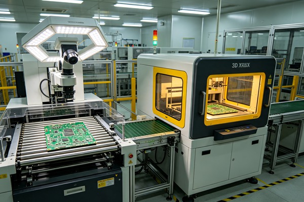
AOI is remarkably fast, routinely capable of fully inspecting a densely populated, large-format motherboard in a matter of seconds. It serves as the high-speed workhorse of the SMT line, handling the heavy lifting of 100% inline inspection for all visible components, polarities, and exposed peripheral joints. 3D X-Ray, inversely, due to the complex physics of radiographic image acquisition and the massive computational load of 3D volume reconstruction, is traditionally slower. Therefore, the optimal, industry-proven strategy is to employ 3D AOI for 100% inline, real-time inspection, subsequently followed by either inline or strategically offline 3D X-Ray specifically targeting only the high-risk, hidden solder joints of BGAs, complex QFNs, and critical power-handling components. Learn more about Via-in-Pad Plated Over (VIPPO): Design Guidelines for Fine-Pitch BGA Breakout.
By intelligently combining the rapid, comprehensive surface-level analysis of 3D AOI with the deep, penetrating internal volumetric analysis of 3D X-Ray, manufacturers effectively achieve complete, uncompromised structural test coverage.
How to Implement AOI and 3D X-Ray (Step-by-Step Guide)
Follow these engineering rules.
- Evaluate PCBA Complexity and Component Mix
Begin by rigorously analyzing the Bill of Materials (BOM) and the specific CAD layout of your PCB designs. Identify the precise ratio and percentage of visible components versus hidden-joint components (BGAs, CSPs, micro-BGAs, QFNs, LGAs). Determine the physical dimensions of the smallest passive components (e.g., 0201, 01005, or even 008004 metric) and the pin pitch of the tightest integrated circuits. This critical evaluation will directly dictate the optical resolution requirements for the AOI camera sensors and the required kV power and focal spot size for the AXI X-Ray tube.
- Integrate AOI Post-Reflow and Pre-Reflow
Deploy your sophisticated 3D AOI systems inline within the SMT flow. Post-reflow AOI is universally mandatory for final visible solder joint validation and overall assembly sign-off. However, if your First Pass Yield (FPY) requires aggressive earlier intervention to reduce rework costs, seriously consider implementing pre-reflow AOI (positioned immediately after the high-speed component placement machines but before the reflow oven). This strategic placement catches placement deviations, missing parts, and wrong-part errors when they are vastly cheaper and easier to rectify—before the solder paste is melted and the defect is permanently solidified.
- Deploy 3D X-Ray for Complex Packages
Based on the defined takt time and overall cycle time of your production line, decide between an inline or offline 3D X-Ray deployment. For high-volume, high-mix lines heavily populated with complex BGAs, an inline AXI system programmed to dynamically inspect only the hidden joints is optimal to maintain line flow. For lower production volumes, highly specialized NPI (New Product Introduction) runs, or complex failure analysis, investing in an advanced, high-resolution offline CT X-Ray system provides unparalleled deep analytical capabilities for batch auditing and root-cause determination.
- Establish a Unified Data Loop for Process Control
Do not allow your multi-million-dollar inspection machines to operate as isolated data silos. Connect both the SPI, AOI, and X-Ray systems to a centralized Manufacturing Execution System (MES) or dedicated factory yield management software suite. Configure intelligent, closed-loop feedback mechanisms so that statistical inspection data trending at the end of the line can automatically alert line operators or proactively adjust upstream machine parameters (such as solder paste printer squeegee pressure, stencil offsets, or pick-and-place nozzle pressures) before hard defect limits are actually breached.
- Train Engineering and QA Personnel
Operating advanced 3D metrology and radiographic equipment requires highly skilled, analytical operators and process programmers. Invest heavily in continuous, comprehensive training for your manufacturing engineering and Quality Assurance (QA) teams. They must deeply understand not only how to efficiently program the machines and tune complex inspection algorithms to minimize false calls, but also how to accurately interpret intricate 3D X-ray volumetric slices and trace identified defect signatures back to their exact root cause within the upstream SMT printing or placement process.
Implementing a resilient, high-yield inspection strategy requires meticulous planning, process characterization, and disciplined execution. Follow this structured guide to successfully integrate advanced AOI and 3D X-Ray systems into your modern manufacturing environment. Learn more about Extreme Thermal Cycling: Reliability Testing and Material Selection for Aerospace PCBs.
Advanced Defect Analysis and Yield Optimization
The ultimate strategic value of integrating networked AOI and 3D X-Ray lies far beyond mere end-of-line defect sorting; its true power resides in enabling continuous yield optimization and process maturity. Modern inspection platforms are increasingly incorporating sophisticated Artificial Intelligence (AI) and deep Machine Learning (ML) algorithms.
AI-driven inference engines can drastically and continuously reduce false-call rates in AOI by autonomously learning the highly acceptable, nuanced variations in perfectly good solder joints over time, adapting to different component vendors without manual reprogramming. In the realm of X-Ray analysis, AI models can autonomously segment, identify, and classify highly complex defect types—such as micro-cracking, subtle head-in-pillow formations, or irregular void clustering—that might easily escape fatigued human visual inspection. By fully utilizing these advanced, data-driven analytical tools, electronics manufacturers can definitively transition from a reactive, costly posture (catching defects after they occur) to a highly proactive, predictive posture (preventing defects before they form), thereby truly realizing the ultimate vision of zero-defect PCB assembly.
Frequently Asked Questions (FAQ)
Traditional 2D AOI uses flat lighting and cameras to analyze 2D contrast, edges, and color, which makes it highly susceptible to false errors induced by shadows, PCB board warpage, and component color lot changes. Modern 3D AOI, conversely, uses structured light projection or lasers to construct a physical, mathematical topographic map of the entire board. This allows for precise, repeatable volumetric measurements of component bodies and solder fillets, significantly reducing false calls and vastly improving measurement accuracy.
No, AOI absolutely cannot reliably inspect BGA solder joints because the technology relies strictly on a direct, unobstructed line-of-sight visual inspection. The critical solder spheres on a BGA are located entirely underneath the opaque component package body, completely hidden from the AOI’s optical cameras. 3D X-Ray is the only non-destructive method required to effectively inspect these hidden internal joints.
3D X-Ray (AXI) captures hundreds of radiographic images through the board at various angles and reconstructs them into a solid 3D digital volume (computed tomography). Because the encapsulated gas trapped within a void is vastly less dense than the surrounding heavy metal solder alloy, it appears as a distinct, lighter area or “empty space” within the X-ray data matrix. The system’s advanced software precisely calculates the internal volume of this empty space relative to the total calculated volume of the surrounding solder joint to determine an exact void percentage.
For manufacturing high-reliability, mission-critical, or complex, dense boards (e.g., medical devices, aerospace avionics, autonomous automotive systems), the answer is a definitive yes. AOI provides rapid, cost-effective 100% surface coverage of visible components and joints, while 3D X-Ray provides the mandatory internal inspection for hidden structural joints (BGAs, QFNs). Strategically deploying both ensures maximum test coverage and aggressively minimizes the risk of catastrophic field failures.
Closed-loop feedback takes the granular defect and measurement data identified by SPI, AOI, and X-Ray systems at various points in the line and automatically networks it back to earlier stages of the manufacturing process (like the initial solder paste printer or the component pick-and-place machine). This sophisticated networking allows the manufacturing system to intelligently correct slight, creeping process drifts (e.g., a stencil alignment slowly shifting out of tolerance) dynamically before those drifts degrade into actual hard defects, thereby continuously optimizing the line’s First Pass Yield (FPY).