In the rapidly evolving landscape of the Internet of Things (IoT), the relentless drive towards miniaturization has fundamentally reshaped electronic design and manufacturing. As consumer and industrial demands converge on smaller, lighter, and more powerful connected devices, traditional Printed Circuit Board (PCB) assembly techniques are reaching their physical limits. Surface Mount Technology (SMT) and Through-Hole Technology (THT) consume critical real estate on the top and bottom layers of a board. To bypass these spatial constraints, forward-thinking engineers are increasingly turning to a transformative approach: embedded PCB components.
By embedding active and passive components directly within the inner layers of a multilayer PCB substrate, designers can reclaim valuable surface area, enhance signal integrity, and achieve unprecedented levels of miniaturization. This article explores the engineering principles, manufacturing processes, and design methodologies associated with embedded components, offering a comprehensive guide for B2B engineering teams aiming to push the boundaries of IoT device miniaturization. Learn more about Via-in-Pad Plated Over (VIPPO): Design Guidelines for Fine-Pitch BGA Breakout.
Table of Contents
Understanding Embedded PCB Components
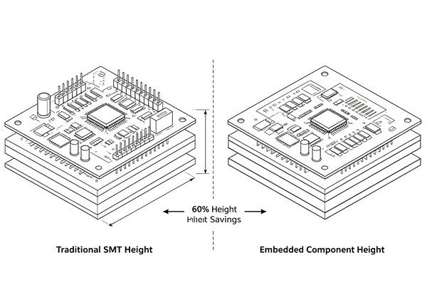
Embedded component technology refers to the integration of electronic components—such as resistors, capacitors, inductors, and even complex integrated circuits (ICs)—directly into the internal layers of a printed circuit board, rather than mounting them on the surface. This technique leverages the Z-axis of the PCB, transforming the substrate from a mere interconnect mechanism into a highly functional module. Learn more about Hard Gold Plating: Edge Connectors and Switch Contacts Design for Extreme Wear Resistance.
Types of Embedded Components
-
Passive Components (Resistors, Capacitors, Inductors): The embedding of passive components is the most mature and widely adopted implementation of this technology. Passive components often account for up to 80% of the total part count on a typical PCB. By moving them into the inner layers, engineers can drastically reduce the required board size.
- Formed Components: These are created directly during the PCB manufacturing process using specialized resistive or capacitive materials deposited onto the inner layers.
- Placed Components: These are discrete, ultra-thin passive components manufactured specifically for embedding and placed into pre-routed cavities or directly on inner layers before lamination.
-
Active Components (ICs, Microcontrollers): Embedding active components, such as bare die or ultra-thin packaged ICs, represents a more complex but highly rewarding frontier. Active embedding is particularly beneficial for IoT edge nodes where minimizing the footprint is critical, and high-frequency signal integrity is paramount.
Engineering Advantages for IoT Miniaturization
The transition from surface-mounted to embedded components offers compelling advantages for IoT device engineering, far beyond simple space savings.
The Manufacturing Process of Embedded PCBs
Manufacturing PCBs with embedded components requires advanced fabrication techniques and tight tolerances. The B2B supply chain for these specialized boards involves close collaboration between the design engineers and the PCB fabricator. There are generally two primary methodologies: the cavity approach and the flat embedding approach.
The Cavity Approach
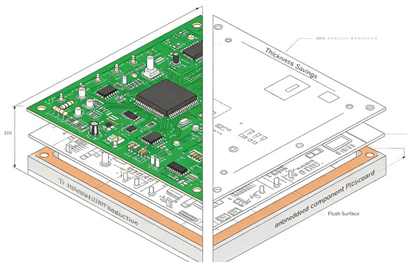
In this method, cavities or pockets are routed or laser-ablated into the core material of the PCB. The discrete components (either active dies or thin passives) are placed into these cavities. The components are then encapsulated with a specialized resin or prepreg material, and the subsequent layers are laminated on top. Vias are then drilled and plated to establish electrical connections to the embedded component’s terminals.
The Flat Embedding Approach (Lamination)
This process is often used for ultra-thin components. The components are placed directly onto an internal copper layer and temporarily secured with an adhesive. A layer of prepreg (resin-impregnated fiberglass) with cutouts, or a highly flowable resin, is placed over them. Under heat and pressure during the lamination cycle, the resin flows around the components, encapsulating them seamlessly. Microvias are subsequently laser-drilled down to the component pads and copper-plated to create the interconnections. Learn more about Crosstalk Mitigation: Advanced Routing Techniques to Minimize NEXT and FEXT in High-Speed PCBs.
Overcoming Engineering Challenges
While the benefits are substantial, embedding components introduces specific engineering and manufacturing challenges that must be navigated.
- Design Complexity: Designing embedded PCBs requires sophisticated EDA (Electronic Design Automation) tools that support 3D design and Z-axis component placement. The routing complexity increases exponentially, requiring careful planning of layer stack-ups and microvia structures.
- Manufacturing Yield and Cost: The fabrication process involves more steps, tighter tolerances, and specialized materials, which inherently increases the initial manufacturing cost and can impact yield rates. A defect in an embedded component renders the entire board useless, as rework is virtually impossible.
- Testing and Inspection: Inspecting embedded components is exceptionally difficult. Traditional Automated Optical Inspection (AOI) cannot see inside the board. Engineers must rely on advanced techniques like X-ray inspection and robust functional testing strategies to ensure quality.
How to Design PCBs with Embedded Components (Step-by-Step Guide)
Follow these engineering rules.
- Unprecedented Space Reduction
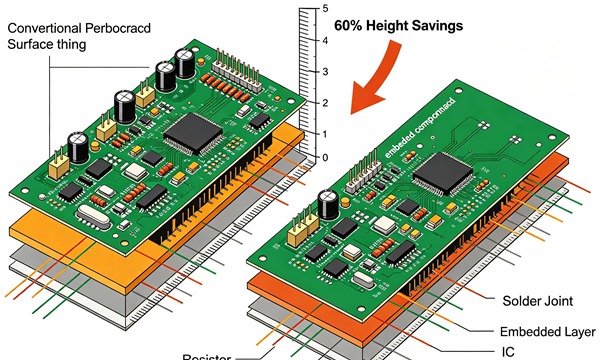
The most immediate and obvious benefit is the dramatic reduction in PCB footprint. By relocating the bulk of passive components and critical active ICs to the internal layers, the external surface area is freed up. This allows for smaller form factors essential for wearables, medical implants, and compact industrial sensors. In many cases, board size can be reduced by 30% to 50%.
- Enhanced Signal Integrity and Parasitic Reduction
In high-speed IoT devices relying on RF communication (such as BLE, Wi-Fi, or 5G), parasitic inductance and capacitance from surface traces and vias can degrade signal integrity. Embedded components significantly shorten the interconnection distance between components. Placing decoupling capacitors directly beneath an IC chip, for example, minimizes trace length, lowers parasitic inductance, and provides cleaner power delivery, which is critical for high-frequency switching.
- Improved Thermal Management
Dissipating heat in miniaturized IoT devices is a constant engineering challenge. Traditional SMT components rely on the surface area and thermal vias to transfer heat. When components are embedded within the substrate, particularly near highly conductive copper planes, the entire PCB acts as a heat sink. The dielectric materials surrounding the embedded components can facilitate better lateral and vertical thermal dissipation, reducing localized hot spots.
- Increased Reliability and Environmental Protection
IoT devices deployed in industrial or outdoor environments face harsh conditions, including moisture, dust, and mechanical vibration. Components embedded within the FR-4 (or other substrate materials) are hermetically sealed and protected from external environmental factors. Furthermore, embedded components are immune to solder joint fatigue caused by thermal cycling or mechanical shock, a common failure mode in traditional surface-mount assemblies.
- Evaluate Project Feasibility and Cost-Benefit
Before committing to embedded technology, conduct a thorough analysis. Determine if the stringent miniaturization, signal integrity, or reliability requirements of your IoT device justify the increased manufacturing costs and design complexity. Consult with your PCB fabricator early to understand their specific capabilities, layer stack-up limitations, and minimum component sizes they can reliably embed.
- Select Appropriate Embedded Components
Not all components are suitable for embedding. Work closely with component manufacturers to source ultra-thin profiles specifically designed for embedding. For passives, consider the trade-offs between formed (printed) resistors/capacitors versus placed discrete components. For active components, ensure you have access to bare dies or low-profile wafer-level chip scale packages (WLCSP) with appropriate pad metallization for microvia plating.
- Define the Layer Stack-Up and Z-Axis Architecture
The layer stack-up is the foundation of embedded design. Decide which internal layers will house the components. This decision impacts routing density, thermal management, and signal integrity. Collaborate with your fabricator to define the core thicknesses, prepreg types, and the required cavity depths to accommodate the Z-height of your selected components without causing bulges or lamination voids.
- Configure EDA Tools for 3D Design
Ensure your PCB layout software supports embedded component design rules. Configure the component libraries to include precise 3D mechanical models and specify which layers the components are permitted to reside on. Set up specific Design Rule Checks (DRC) for embedded components, including clearance around cavities, microvia aspect ratios, and keep-out zones on adjacent layers.
- Execute Strategic Component Placement
Begin placement by positioning the critical embedded components. For high-speed or RF IoT applications, place decoupling capacitors directly beneath the associated active ICs to minimize parasitic inductance. Ensure adequate spacing between embedded components to allow for the flow of resin during lamination and to maintain structural integrity of the core material.
- Route Microvias and Interconnections
Routing embedded components relies heavily on microvia technology. Route laser-drilled blind or buried vias to connect the inner-layer component pads to the necessary power, ground, and signal layers. Pay meticulous attention to via pad sizes, laser drill registration tolerances, and plating requirements to ensure robust electrical connections to the embedded terminals.
- Implement Thermal Management Strategies
Since embedded components are encapsulated in dielectric materials, heat dissipation must be carefully managed. Utilize solid copper planes adjacent to the embedded layers to act as heat spreaders. Implement thermal vias strategically to conduct heat away from embedded high-power active components towards the outer layers where heat sinks or forced air cooling can be applied.
- Develop a Comprehensive Testing Strategy
Because embedded components cannot be physically probed or optically inspected after manufacturing, testing must be designed into the board. Implement boundary scan (JTAG) for digital ICs. Design comprehensive functional test procedures that can infer the operational status of embedded passive networks and active chips based on external I/O behavior.
Designing a PCB with embedded components requires a paradigm shift from traditional 2D layout strategies to a comprehensive 3D co-design approach. Follow these critical steps to ensure a successful implementation. Learn more about IC Substrates: The Evolution of PCB Manufacturing: Introduction to IC Substrates.
Conclusion
Embedded PCB component technology represents a critical leap forward in electronic engineering, providing the necessary tools to meet the relentless demand for miniaturization in the IoT sector. While the design and manufacturing processes are significantly more complex than traditional surface-mount methods, the advantages—reduced footprint, superior signal integrity, enhanced thermal performance, and rugged reliability—are indispensable for next-generation devices. By mastering the engineering principles and adopting advanced design methodologies, B2B engineering teams can leverage embedded components to create innovative, highly integrated IoT solutions that define the future of connectivity.
Frequently Asked Questions (FAQ)
No, once a component is embedded and the PCB is laminated, it is permanently sealed within the substrate. Rework or replacement is impossible. This makes stringent quality control during manufacturing and robust upfront design absolutely critical, as a single component failure renders the entire board defective.
The cost increase varies widely depending on the complexity, layer count, and whether you are embedding active or passive components. Generally, expect a 20% to 50% premium over a standard multi-layer SMT board. However, this increased PCB cost can sometimes be offset by reduced assembly costs, smaller enclosures, and improved system-level performance.
Typically, no. Standard SMT components are often too thick for internal layers and have terminations designed for solder paste, not for microvia plating. Embedded designs require specialized low-profile components or bare dies. For passives, manufacturers offer ultra-thin parts specifically designed for the lamination and via-in-pad plating processes used in embedding.
Thermal management must be integrated into the PCB design. This is achieved by utilizing heavy copper inner layers as heat spreaders directly adjacent to the embedded component, and by using arrays of thermal vias to conduct heat from the embedded IC to the outer surface of the board, where it can be dissipated to the environment or a heat sink.