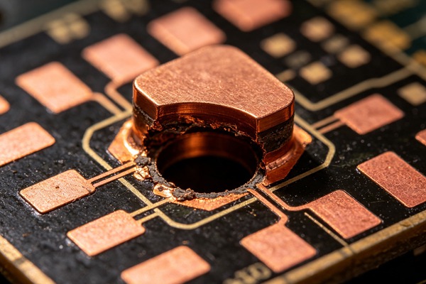
As electronic devices continue to shrink while their computational capabilities expand, Printed Circuit Board (PCB) designers are constantly challenged to route highly complex circuits within increasingly constrained footprints. One of the most significant bottlenecks in modern High-Density Interconnect (HDI) PCB design is the breakout and routing of fine-pitch Ball Grid Arrays (BGAs). When BGA pin pitches drop below 0.5mm, traditional routing techniques, such as the standard dog-bone fanout, simply run out of physical space.
To address this spatial limitation and maintain signal integrity, PCB engineers turn to advanced via technologies. Foremost among these solutions is Via-in-Pad Plated Over (VIPPO). By placing the via directly within the surface mount pad and plating over it to create a flat, solderable surface, VIPPO allows for direct vertical routing. This comprehensive guide explores the structural mechanics of VIPPO, compares it with conventional methodologies, and provides detailed design guidelines for successfully implementing VIPPO in fine-pitch BGA breakouts.
Table of Contents
The Challenge of Fine-Pitch BGA Breakout
Modern microprocessors, FPGAs, and high-speed ASICs often employ BGA packages to maximize pin count within a minimal area. While 1.0mm and 0.8mm pitch BGAs offer sufficient space for trace routing between pads using conventional through-hole vias, fine-pitch BGAs—typically categorized as having pitches of 0.5mm, 0.4mm, or even smaller—present a formidable routing challenge. Learn more about Hard Gold Plating: Edge Connectors and Switch Contacts Design for Extreme Wear Resistance.
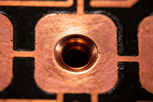
The primary issue lies in the geometric constraints. In a traditional dog-bone fanout, a short trace connects the BGA pad to an adjacent via. However, as the pitch decreases, the clearance between the BGA pads shrinks. Eventually, there is insufficient room to place a via between the pads or to route a trace between them without violating the minimum trace-to-trace or trace-to-pad clearance requirements dictated by the manufacturer’s Design Rule Checks (DRC).
Furthermore, high-speed digital designs require stringent control over signal integrity. The short trace in a dog-bone fanout introduces parasitic inductance and capacitance, which can degrade high-frequency signals and cause impedance discontinuities. Therefore, a solution that eliminates this stub, minimizes the routing footprint, and supports high-density interconnect architectures is strictly required for advanced applications. Learn more about Conformal Coating: Protecting PCBA from Moisture, Dust, and Corrosive Environments.
Understanding Via-in-Pad Plated Over (VIPPO)
Via-in-Pad Plated Over (VIPPO), sometimes referred to as Plated Over Filled Via (POFV), is a specialized via manufacturing process where a via is drilled directly inside the copper pad intended for a surface mount component, typically a BGA.
The standard via-in-pad process simply leaves the via hole open within the pad. While this saves space, it introduces a critical manufacturing defect during the assembly phase: solder wicking. During reflow soldering, the capillary action of the open via draws the liquid solder away from the component pad and down into the via barrel. This results in solder-starved joints, poor mechanical adhesion, and a high probability of electrical opens or unreliable connections.
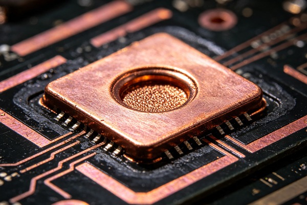
VIPPO mitigates this problem entirely through a multi-step manufacturing process:
1. Drilling and Plating: The via is mechanically or laser drilled and plated to establish electrical connectivity between the layers.
2. Epoxy Fill: The via barrel is completely filled with a specialized epoxy resin. This resin can be either conductive or non-conductive, depending on the thermal and electrical requirements of the design.
3. Planarization: After the via is filled and cured, the surface is planarized (sanded flat) to remove any excess resin.
4. Plating Over: Finally, a layer of copper is plated directly over the filled via, creating a completely flat, uninterrupted, and highly solderable pad surface.
The final result is a pad that looks and behaves exactly like a standard surface mount pad during the assembly process but contains a direct, vertical interconnect to the inner layers of the PCB.
VIPPO vs. Traditional Dog-Bone Fanout
While the traditional dog-bone fanout is cost-effective and suitable for larger pitch components, its utility diminishes rapidly in HDI designs. The dog-bone structure consumes valuable surface real estate, limiting the number of bypass capacitors or other passive components that can be placed on the opposite side of the board directly beneath the BGA.
Conversely, VIPPO consolidates the pad and the via into a single physical entity. This eliminates the need for breakout traces on the surface layer, freeing up routing channels and drastically simplifying the BGA fanout. Furthermore, because VIPPO provides a direct vertical path from the component pin to the internal routing layer, it significantly reduces parasitic inductance. This direct path is highly advantageous for high-speed signal integrity and for minimizing the impedance in power distribution networks (PDNs), allowing decoupling capacitors to be placed directly underneath the BGA via for maximum effectiveness.
Design Guidelines for VIPPO Implementation
Successfully integrating VIPPO into a PCB design requires careful adherence to specific design parameters and close collaboration with the fabrication house. The following guidelines outline the critical specifications for VIPPO implementation.
Aspect Ratio and Drill Sizes
The aspect ratio—the ratio of the PCB thickness to the drilled hole diameter—is a crucial factor in reliable via plating and filling. For standard mechanical drilling, a maximum aspect ratio of 10:1 is generally recommended, though 8:1 is safer for ensuring consistent copper plating in the via barrel. When using laser-drilled microvias for VIPPO in HDI buildups, the aspect ratio is typically constrained to 1:1 or 0.8:1.
For a standard 1.6mm (63 mil) thick board, the minimum mechanical drill size should typically not fall below 0.15mm (6 mil) or 0.2mm (8 mil) to maintain a reliable aspect ratio and allow for proper epoxy filling.
Pad Size and Annular Ring Requirements
The BGA pad size is dictated by the component manufacturer’s recommendations, usually ranging from 80% to 100% of the BGA sphere diameter. When implementing VIPPO, you must ensure that the pad is large enough to accommodate the drilled via while leaving a sufficient annular ring. A minimum annular ring of 0.1mm (4 mils) is the industry standard to account for drill wander and registration tolerances during manufacturing. For example, if the BGA pad is 0.4mm (16 mils), the maximum via drill size should be 0.2mm (8 mils).
Epoxy Fill Material: Conductive vs. Non-Conductive
The choice between conductive and non-conductive epoxy fill is a frequent point of confusion. In the vast majority of applications, non-conductive epoxy is the preferred choice. Non-conductive epoxy has a coefficient of thermal expansion (CTE) that closely matches that of the surrounding FR4 substrate, reducing the risk of via barrel cracking during thermal cycling. The electrical and thermal conductivity in a non-conductive filled via is provided entirely by the copper plated on the via walls.
Conductive epoxy is generally reserved for specialized applications requiring extreme thermal dissipation directly through the via, as its CTE mismatch can cause reliability issues over time. Learn more about Flying Probe vs. ICT: Choosing the Right PCBA Testing Strategy for Your Production Volume.
How to Implement VIPPO (Step-by-Step Guide)
Follow these engineering rules.
- Assess BGA Pitch and Routing Density
Begin by analyzing the pin pitch of your chosen BGA. If the pitch is 0.5mm or below, VIPPO is highly recommended, if not mandatory. Evaluate the layer count and determine if standard through-hole VIPPO is sufficient or if stacked microvias (HDI) with VIPPO will be necessary to achieve the required routing density.
- Define Via and Pad Dimensions
Consult the component datasheet to establish the optimal pad size. Calculate the maximum allowable drill size by subtracting the required annular ring (typically 0.1mm per side) from the pad diameter. Ensure this drill size satisfies the fabricator’s aspect ratio limits based on the board thickness.
- Select the Appropriate Fill Material
Specify the use of non-conductive epoxy fill for the vias unless there is an extreme thermal requirement that necessitates conductive fill. Document this clearly in your fabrication notes to avoid assumptions by the manufacturer.
- Specify the Plating and Surface Finish
Indicate that the vias must be planarized and plated over with copper. Following the copper plating, specify a reliable surface finish. Electroless Nickel Immersion Gold (ENIG) or Electroless Nickel Electroless Palladium Immersion Gold (ENEPIG) are highly recommended for fine-pitch BGAs due to their excellent planarity and oxidation resistance.
- Verify Design with DRC and Manufacturer
Update your EDA software’s Design Rule Check (DRC) parameters to allow vias to intersect with surface mount pads without throwing errors. Before releasing the Gerber files, send a preliminary stackup and via definition to your PCB manufacturer to confirm that their equipment can reliably produce the specified VIPPO dimensions according to IPC-4761 Type VII standards.
Transitioning to a VIPPO routing strategy requires a systematic approach to ensure manufacturability and reliability. Learn more about Burn-in Boards (BIB): Designing High-Temperature Burn-In Boards for Semiconductor Testing.
Reliability and Manufacturing Considerations
While VIPPO solves complex routing problems, it introduces new variables into the manufacturing process. The primary concern is thermal reliability. Because the via contains materials with different CTEs (copper, epoxy fill, and FR4 substrate), repeated thermal cycling during operation or reflow can induce stress on the via barrel and the plated cap. Over time, this stress can lead to micro-cracks in the copper plating or separation of the cap from the via, resulting in intermittent failures.
To mitigate these risks, manufacturers must control the planarization process precisely. If the epoxy is not perfectly flush with the copper pad before the final plating over, a “dimple” or a “bump” will form on the pad surface. A dimple can trap flux and outgas during reflow, causing solder voids within the BGA joint. A bump can cause the BGA to sit unevenly, leading to open circuits on adjacent pins. IPC-4761 standardizes the design and classification of via protection. For true VIPPO, you must strictly specify IPC-4761 Type VII (Filled and Capped) in your manufacturing notes.
Conclusion
Via-in-Pad Plated Over (VIPPO) is an indispensable technology for modern PCB engineers dealing with high-pin-count, fine-pitch BGA components. By eliminating the need for space-consuming dog-bone fanouts, VIPPO maximizes routing channels, enhances signal integrity, and optimizes power distribution networks. While it requires adherence to strict design rules and adds manufacturing complexity and cost, the benefits in miniaturization and performance make it a mandatory technique for high-density interconnect designs.
Frequently Asked Questions (FAQ)
Yes. The VIPPO process requires several additional manufacturing steps compared to standard vias, including filling, curing, planarization, and a secondary plating cycle. This typically increases the bare board fabrication cost by 15% to 30%, depending on the manufacturer and the complexity of the board.
For BGA pads, it is highly discouraged. Leaving a via open within a pad will cause solder wicking during assembly, where the solder meant for the BGA joint flows down into the via hole. This invariably leads to weak, unreliable, or completely open connections. VIPPO is required to prevent this phenomenon.
In most standard and HDI designs, non-conductive epoxy is highly recommended. It matches the thermal expansion properties of the PCB substrate better than conductive epoxy, reducing the risk of via cracking during thermal cycles. The copper plating on the via walls provides adequate electrical and thermal conductivity.
ENIG (Electroless Nickel Immersion Gold) and ENEPIG (Electroless Nickel Electroless Palladium Immersion Gold) are the preferred surface finishes. They provide an exceptionally flat and uniform surface, which is critical for the reliable seating and soldering of fine-pitch BGA components.
No, although they are often used together in HDI designs. A microvia is defined by its small size (typically <= 0.15mm diameter) and low aspect ratio, usually spanning only one dielectric layer. VIPPO is a process applied to a via (which could be a microvia or a standard through-hole via) where it is filled and plated over to create a flat pad surface.