Table of Contents
Introduction to Ceramic Substrates in High-Power Electronics
In modern electronics engineering, pushing the boundaries of power density, miniaturization, and operating temperatures has rendered traditional substrate materials like FR4 increasingly obsolete for high-stress applications. When designing power electronics, high-brightness LEDs, RF/microwave systems, and automotive powertrain modules, the primary cause of system failure is typically thermal mismanagement. If heat is not rapidly and efficiently extracted from active semiconductor junctions, the resulting thermal runaway can lead to catastrophic component failure, solder joint fatigue, and reduced mean time between failures (MTBF).
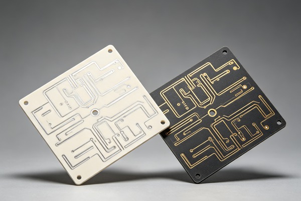
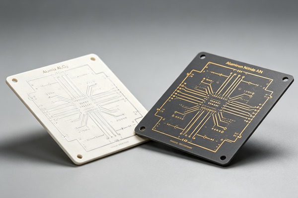
To combat these extreme thermal loads, engineers frequently turn to ceramic printed circuit boards (PCBs). Unlike organic substrates, ceramic boards offer a unique combination of exceptional thermal conductivity, outstanding electrical insulation (high dielectric strength), and a low coefficient of thermal expansion (CTE) that closely matches that of bare semiconductor dies (like Silicon, Silicon Carbide, and Gallium Nitride). Among the various ceramic materials available, two dominate the industry: Alumina (Al2O3) and Aluminum Nitride (AlN).
While both provide significant upgrades over standard FR4 and Metal Core PCBs (MCPCBs), they cater to very different tiers of performance and budget constraints. Understanding the thermomechanical properties, manufacturing nuances, and application suitability of Alumina versus Aluminum Nitride is essential for any hardware engineer looking to optimize a high-power electronic assembly. This comprehensive guide will dissect the characteristics of both materials, compare them across critical engineering metrics, and provide a step-by-step approach to selecting the right ceramic PCB for your extreme heat applications.
The Limitations of Traditional PCBs and the Rise of Ceramics
Before delving into the specifics of Alumina and AlN, it is crucial to understand why ceramic substrates are specified in the first place. Standard FR4 has a thermal conductivity of roughly 0.25 to 0.35 W/m·K. It acts as an excellent thermal insulator, which is exactly the opposite of what is required in power electronics. Heat generated by surface-mounted devices gets trapped, causing junction temperatures to skyrocket. Learn more about Return Path Optimization: Designing Solid Reference Planes for High-Frequency Signal Integrity.
Metal Core PCBs (MCPCBs), typically using an aluminum or copper backing, improve upon this by offering thermal conductivities in the range of 1.0 to 7.0 W/m·K (depending on the dielectric layer). However, MCPCBs have a critical flaw for high-voltage, extreme-power applications: the thermal bottleneck is the organic dielectric layer separating the copper circuit from the metal core. This layer has limited thermal transfer capabilities and is susceptible to dielectric breakdown at high voltages.
Ceramic PCBs eliminate this bottleneck entirely. In a ceramic PCB, the ceramic material itself acts as both the structural base and the electrical insulator. Because ceramics are inherently excellent electrical insulators, there is no need for an intermediate organic dielectric layer. The conductive copper or silver traces are bonded directly to the ceramic substrate. This direct bonding minimizes thermal resistance, allowing heat to flow seamlessly from the component through the substrate to the heat sink. Furthermore, ceramics boast a low CTE (around 4.5 to 7.5 ppm/°C), which drastically reduces the thermomechanical stress placed on solder joints during rapid thermal cycling, a frequent cause of failure in harsh environments. Learn more about Crosstalk Mitigation: Advanced Routing Techniques to Minimize NEXT and FEXT in High-Speed PCBs.
Alumina (Al2O3) Ceramic PCBs: The Industry Workhorse
Alumina, or Aluminum Oxide (Al2O3), is the most widely used ceramic substrate material in the electronics industry, accounting for the vast majority of ceramic PCB production. It is favored because it strikes an excellent balance between thermal performance, mechanical strength, and cost-effectiveness.
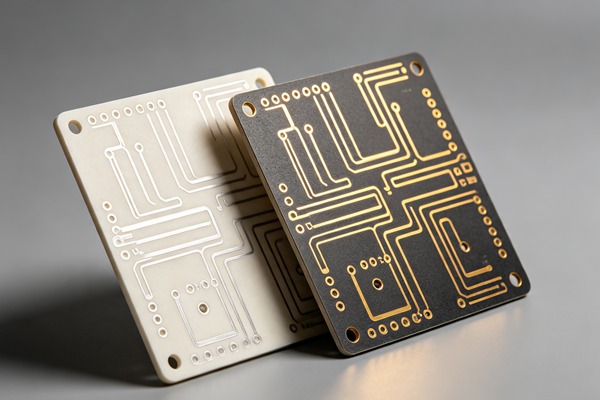
Typically available in purities ranging from 96% to 99.6%, Alumina offers a thermal conductivity of approximately 18 to 36 W/m·K. While this might seem modest compared to pure metals, it is roughly 100 times better than FR4 and vastly superior to most MCPCB dielectric layers.
Key Characteristics of Alumina PCBs:
- Thermal Conductivity: At 24-36 W/m·K (for 96% purity), Alumina efficiently handles moderate to high heat loads, making it suitable for a wide array of power modules and LED applications.
- Mechanical Integrity: Alumina is exceptionally hard and rigid. It possesses high flexural strength, making it durable during the manufacturing and assembly processes.
- Cost-Effectiveness: Compared to advanced ceramics like AlN or Beryllium Oxide (BeO), Alumina is relatively inexpensive to procure and process. The raw materials are abundant, and the sintering and metallization processes are highly mature and standardized across the global supply chain.
- Dielectric Properties: It exhibits excellent dielectric strength (typically >15 kV/mm), allowing for high-voltage isolation in power converters and motor drives.
- Chemical Stability: Alumina is highly resistant to chemical corrosion and does not degrade in harsh, reactive environments, ensuring long-term reliability in automotive and industrial settings.
Common Applications for Alumina:
Alumina is the default choice for standard power electronics, automotive sensors, Peltier coolers (thermoelectric modules), thick-film hybrid circuits, and general-purpose high-brightness LED lighting arrays. It is the pragmatic engineer’s choice when FR4 fails, but the extreme costs of AlN cannot be justified.
Aluminum Nitride (AlN) Ceramic PCBs: The High-Performance Apex
For applications where thermal loads reach extreme levels—such as in concentrated photovoltaics, high-power lasers, and next-generation wide-bandgap (WBG) semiconductor modules—Alumina’s thermal conductivity is insufficient. Enter Aluminum Nitride (AlN).
Aluminum Nitride is an advanced ceramic compound engineered specifically for extreme thermal management. It boasts a staggering thermal conductivity ranging from 170 W/m·K to over 220 W/m·K. To put this in perspective, AlN’s thermal conductivity is nearly 7 to 10 times higher than that of Alumina, and it approaches the thermal conductivity of metallic aluminum (which is ~210 W/m·K), but without the electrical conductivity.
Key Characteristics of AlN PCBs:
- Exceptional Thermal Conductivity: With ratings between 170-220 W/m·K, AlN is the premier choice for rapidly drawing heat away from dense, high-power semiconductor junctions. It prevents localized hot spots that can degrade component lifespan.
- Optimal CTE Matching: AlN has a coefficient of thermal expansion of approximately 4.5 ppm/°C. This perfectly matches the CTE of Silicon (Si) and closely aligns with Silicon Carbide (SiC) and Gallium Nitride (GaN). This exact match minimizes thermal expansion mismatch, drastically reducing shear stress on bare dies and solder joints during extreme thermal cycling.
- High Dielectric Strength: Like Alumina, AlN is a superb electrical insulator, capable of isolating high voltages (typically >15 kV/mm), which is critical for high-power IGBTs and MOSFETs.
- Non-Toxic Alternative: Historically, Beryllium Oxide (BeO) was used for extreme thermal applications. However, BeO dust is highly toxic and poses severe health risks during machining. AlN offers similar thermal performance to BeO but is entirely non-toxic and environmentally safe.
- Higher Cost and Complexity: The primary drawback of AlN is its cost. The raw powder synthesis is complex, and the high-temperature sintering process (often requiring Yttria as a sintering aid) is energy-intensive. Furthermore, metallizing AlN requires specialized techniques, driving up the total PCB fabrication cost.
Common Applications for AlN:
AlN is strictly specified for mission-critical, extreme-heat environments. Typical use cases include high-power Insulated Gate Bipolar Transistor (IGBT) modules for electric vehicles and rail traction, high-power RF and microwave amplifiers, military and aerospace radar systems, deep-UV LEDs, and laser diode mounts. Learn more about Flying Probe vs. ICT: Choosing the Right PCBA Testing Strategy for Your Production Volume.
Head-to-Head Engineering Comparison: Alumina vs. AlN
To facilitate a quantitative engineering decision, the table below highlights the comparative material properties of standard 96% Alumina and typical Aluminum Nitride substrates.
| Property / Metric | Alumina (Al2O3 – 96%) | Aluminum Nitride (AlN) | Engineering Implication |
|---|---|---|---|
| Thermal Conductivity (W/m·K) | 24 – 36 | 170 – 220 | AlN extracts heat up to 10x faster, vital for dense power modules. |
| Coefficient of Thermal Expansion (ppm/°C) | 6.5 – 7.5 | 4.5 – 5.5 | AlN matches Silicon (4.0 ppm/°C) better, reducing solder fatigue. |
| Dielectric Strength (kV/mm) | ~ 15 | > 15 | Both provide excellent high-voltage electrical isolation. |
| Flexural Strength (MPa) | 300 – 400 | 280 – 350 | Alumina is slightly more robust mechanically against bending. |
| Dielectric Constant (@ 1 MHz) | 9.0 – 10.0 | 8.5 – 9.0 | AlN has marginally better properties for high-frequency RF signaling. |
| Cost Profile | Low to Moderate | High | Alumina is cost-effective; AlN is reserved for extreme necessity. |
| Machinability | Moderate | Difficult (brittle) | AlN requires specialized laser drilling and routing parameters. |
How to Select and Design for Ceramic PCBs (Step-by-Step Guide)
Follow these engineering rules. Learn more about Press-Fit Connectors: PCB Manufacturing Tolerances for Solderless Interconnects.
- Evaluate Thermal Requirements and Heat Dissipation Needs
Calculate the total power dissipation of your circuit and determine the maximum allowable junction temperature (Tj) of your most critical components. Use thermal simulation software (like ANSYS or Flotherm) to model the heat flux. If the simulated thermal resistance of an Alumina board results in junction temperatures exceeding your safe operating area, you must upgrade to Aluminum Nitride (AlN) to ensure rapid heat extraction.
- Match the Coefficient of Thermal Expansion (CTE)
Analyze the packaging of your components. If you are attaching bare semiconductor dies (flip-chip or wire-bonded) directly to the substrate, a CTE mismatch will cause sheer stress during thermal cycling, leading to delamination or solder cracking. Silicon dies have a CTE of ~4.0 ppm/°C. AlN (4.5 ppm/°C) is a near-perfect match and should be selected for direct die attachment. If you are using pre-packaged SMDs with compliant leads, Alumina’s CTE (7.0 ppm/°C) is usually acceptable.
- Determine Mechanical and Structural Constraints
Assess the physical environment of the PCB. Ceramic boards are inherently brittle. If the assembly will be subjected to high levels of mechanical shock or vibration, realize that Alumina generally offers slightly higher flexural strength than AlN. Design your enclosures with proper shock absorption, avoid large continuous spans of ceramic without support, and ensure mounting hardware does not induce bending stress on the brittle substrate.
- Choose the Metallization Process
Select the appropriate metallization technology based on your current-carrying requirements and trace resolution needs. For very high continuous currents (e.g., motor drives), choose Direct Bonded Copper (DBC) or Active Metal Brazing (AMB), which bond thick copper layers (up to 800µm) to the ceramic. AMB is particularly recommended for AlN due to superior adhesion strength. For high-density, fine-pitch routing (e.g., RF circuits or sensors), specify Direct Plated Copper (DPC) or Thin-Film technology, which provides exceptional trace precision but thinner copper weights.
- Assess the Cost vs. Performance Trade-off
Perform a strict cost-benefit analysis. Aluminum Nitride PCBs can cost 3 to 5 times more than Alumina PCBs of the same dimensions. Only specify AlN if the thermal analysis (Step 1) or the bare-die CTE matching requirements (Step 2) absolutely demand it. For the vast majority of standard power LED and commercial power supply applications, Alumina provides a perfectly adequate and economically viable thermal solution.
Choosing the correct ceramic substrate and designing the board requires a systematic approach to balance thermal demands against mechanical and financial constraints.
Metallization Technologies for Ceramic PCBs
The performance of a ceramic PCB is heavily dictated by how the conductive copper layer is bonded to the bare ceramic substrate. Understanding these processes is critical for hardware engineers:
- Direct Bonded Copper (DBC): Copper foil is bonded to the ceramic under high heat and pressure in an oxygen-controlled environment, forming a eutectic melt that adheres the metals. DBC is excellent for thick copper (up to 30 oz) and high current carrying capacity. However, DBC on AlN can suffer from thermal cycling reliability issues if not processed carefully.
- Active Metal Brazing (AMB): This process uses an active metal filler (like Titanium or Zirconium) to chemically bond the copper to the ceramic. AMB provides significantly higher peel strength and thermal cycling reliability than DBC, especially for Aluminum Nitride (AlN) substrates used in extreme automotive (EV) traction inverters.
- Direct Plated Copper (DPC): This process utilizes a vacuum sputtering technique (PVD) to deposit a thin titanium seed layer, followed by electroplating copper to the desired thickness. DPC provides highly accurate, extremely flat, and fine-pitch traces, making it ideal for RF/microwave applications and high-density LED arrays.
- Thick Film Technology: Conductive pastes (silver or gold) are screen-printed onto the ceramic and fired in a high-temperature furnace. This is a highly mature and cost-effective process, but it is generally limited to lower current applications compared to DBC or AMB.
Frequently Asked Questions (FAQ)
The primary difference is thermal conductivity. Aluminum Nitride (AlN) has a thermal conductivity of 170-220 W/m·K, which is roughly 7 to 10 times higher than Alumina (24-36 W/m·K). Additionally, AlN has a lower Coefficient of Thermal Expansion (CTE) that more closely matches bare silicon dies, making it superior for extreme heat and bare-die packaging applications.
FR4 is a thermal insulator and will fail in extreme heat applications. Metal-Core PCBs (MCPCBs) are better, but their thermal performance is bottlenecked by the organic dielectric layer. Ceramic PCBs eliminate this dielectric layer entirely, allowing direct bonding of copper to the thermally conductive ceramic, providing significantly lower thermal resistance and higher voltage isolation.
Yes, AlN PCBs are significantly more expensive—often 3 to 5 times the cost of Alumina. This is due to the complex, energy-intensive manufacturing process required to synthesize AlN powder, the use of expensive sintering aids, and the more difficult metallization processes required to bond copper to AlN compared to Alumina.
Direct Bonded Copper (DBC) bonds thick copper foils to the ceramic using a high-temperature eutectic melting process, making it ideal for carrying massive currents in power modules. Direct Plated Copper (DPC) uses vacuum sputtering and electroplating to create highly precise, fine-pitch traces with excellent surface flatness, making it the preferred choice for high-frequency RF circuits and dense microelectronics.
Because of its high cost and extreme thermal performance, AlN is reserved for the most demanding applications. Common uses include high-power Insulated Gate Bipolar Transistor (IGBT) and Silicon Carbide (SiC) modules for electric vehicles, deep-UV LED arrays, military radar systems, high-power laser diode sub-mounts, and advanced RF/microwave telecommunication amplifiers.