Table of Contents
Introduction to IC Substrates
In the highly specialized field of semiconductor manufacturing and electronics assembly, the integrated circuit (IC) substrate serves as the critical electrochemical and thermomechanical interface between a bare silicon die and the main printed circuit board (PCB). As semiconductor technology scales down to the single-digit nanometer nodes, the discrepancy in scale between the microscopic I/O pads on a silicon chip and the macroscopic traces on a standard motherboard has grown exponentially. The IC substrate exists precisely to bridge this dimensional gap.
An IC substrate is fundamentally a highly advanced, ultra-miniaturized printed circuit board. It acts as the foundational carrier within an IC package, routing power and signals to and from the die, providing mechanical stability, and dissipating thermal energy generated by high-performance silicon. Without the continuous evolution of IC substrates, modern computing paradigms—from high-performance computing (HPC) clusters and artificial intelligence (AI) accelerators to 5G mobile processors—would be entirely unfeasible. This article delves into the technical evolution of PCB manufacturing that led to the modern IC substrate, examining its materials, complex manufacturing processes, and its indispensable role in the future of advanced heterogeneous packaging.
The Evolution of PCB Manufacturing
The trajectory of printed circuit board manufacturing has been one of continuous miniaturization, ruthlessly driven by the demands of Moore’s Law and the need for higher interconnect density. Initially, electronic assemblies relied on through-hole technology (THT), where components with large wire leads were inserted into drilled holes on a board. As integrated circuits became more complex, THT gave way to Surface Mount Technology (SMT). SMT allowed components to be soldered directly onto the surface of the board, significantly reducing parasitic inductance and increasing component density by eliminating the need for large through-holes.
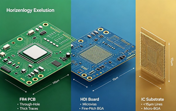
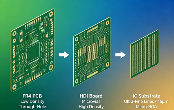
However, as pin counts exploded with the advent of complex microprocessors, standard SMT PCBs could no longer route the necessary density of signals. This limitation necessitated the development of High-Density Interconnect (HDI) PCBs. HDI introduced laser-drilled microvias, blind vias, and buried vias, alongside much finer line widths and spaces (L/S).
The transition from peripheral wire bonding to area-array flip-chip packaging was the definitive catalyst for the modern IC substrate. In a flip-chip configuration, the silicon die is inverted, and its surface I/O pads connect directly to the substrate via microscopic solder bumps. This approach drastically reduced signal path lengths and improved power delivery networks (PDN), but it required a carrier board with trace densities far exceeding what traditional HDI PCB manufacturing could achieve. Thus, the IC substrate emerged as a specialized discipline, fundamentally combining PCB panel-level manufacturing techniques with semiconductor wafer-level cleanroom processes.
Key Differences Between Standard PCBs and IC Substrates
While both standard motherboards and IC substrates utilize conductive copper traces and insulating dielectric layers to route electrical signals, the similarities largely end there. The distinction lies in the extreme miniaturization of their features, the organic materials employed, and the highly controlled manufacturing methodologies.
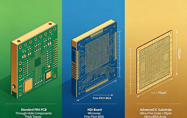
Line Width and Spacing (L/S): A typical advanced HDI PCB might feature line widths and spaces down to 40 micrometers (µm). In stark contrast, modern IC substrates routinely demand L/S parameters of 15/15 µm, 10/10 µm, and in advanced semiconductor nodes, sub-5 µm features are becoming standard to support massive I/O densities.
Vias and Interconnects: Standard PCBs frequently use mechanically drilled vias, usually no smaller than 150 µm in diameter. IC substrates rely almost exclusively on laser-drilled microvias, often in the range of 30 to 50 µm. These microvias are frequently copper-filled via specialized electroplating baths to ensure robust electrical and thermal pathways between ultra-thin dielectric layers without causing voiding. Learn more about Precision Impedance Control: How to Achieve ±5% Impedance Tolerance in High-Speed PCBs.
Dimensional Stability and Tolerance: Because IC substrates must align directly with the microscopic bumps on a rigid silicon die, their dimensional stability tolerances are microscopic. Any warpage caused by coefficient of thermal expansion (CTE) mismatch between the silicon die, the organic substrate, and the motherboard can lead to catastrophic solder joint fatigue and failure during thermal cycling.
Core Materials in IC Substrate Manufacturing
The stringent thermomechanical and high-frequency electrical requirements of advanced IC packaging prohibit the use of standard FR-4 fiberglass laminates in high-performance substrates. Instead, the industry relies on highly engineered specialized organic resins.
Bismaleimide Triazine (BT) Resin: Developed heavily by Mitsubishi Gas Chemical, BT resin is a staple for memory packaging, MEMS, and mobile processors. It offers a high glass transition temperature (Tg), excellent thermal stability, and a relatively low dielectric constant. It is typically utilized for wire-bonded substrates and less complex flip-chip packages where cost is a driving factor.
Ajinomoto Build-up Film (ABF): ABF is the foundational cornerstone of high-performance computing (HPC), CPU, and GPU packaging. It is an epoxy-based film that can be laminated sequentially without the need for fiberglass reinforcement. The absence of glass fibers allows for incredibly fine, homogenous laser drilling and highly predictable fine-line copper etching. This makes ABF the de facto standard for massive, complex flip-chip ball grid array (FCBGA) substrates.
Polyimide (PI): Often used in flex-rigid substrates and specialized applications requiring extreme thermal resistance and flexibility, polyimide is frequently utilized in tape automated bonding (TAB) and chip-on-film (COF) packages for display drivers.
Types of IC Substrates
IC substrates are broadly categorized by the die attach packaging technology they support and their internal structural design. Learn more about Crosstalk Mitigation: Advanced Routing Techniques to Minimize NEXT and FEXT in High-Speed PCBs.
Wire Bonding (WB) IC Substrates: These substrates are designed for traditional packaging where gold, silver, or copper wires connect the die’s peripheral pads to the substrate. While considered a mature, legacy technology, WB substrates are still heavily utilized in cost-sensitive IoT applications, NAND/DRAM memory modules, and analog integrated circuits.
Flip Chip (FC) IC Substrates: FC substrates are specifically engineered for dies that are inverted and bonded directly to the substrate via microscopic solder bumps (C4 bumps). They require significantly higher routing density, highly planar surfaces, and tighter CTE control to prevent bump cracking. FCBGA (Flip Chip Ball Grid Array) and FCCSP (Flip Chip Chip Scale Package) are the primary industry formats.
Coreless Substrates: Traditional substrates are built symmetrically around a rigid, fully cured copper-clad laminate (CCL) core. Coreless substrates entirely eliminate this central core. Instead, they build up dielectric and copper layers sequentially on a temporary carrier plate that is later removed. This architecture allows for significantly thinner overall packages, superior signal integrity at high gigahertz frequencies, and finer routing. However, it introduces immense manufacturing challenges regarding warpage control during assembly. Learn more about AOI & 3D X-Ray: Achieving Zero-Defect PCB Assembly.
How to Manufacture IC Substrates (Step-by-Step Guide)
Follow these engineering rules. Learn more about BGA Underfill: Enhancing PCBA Reliability Against Mechanical Shock and Thermal Stress.
- Material Selection and Core Preparation
The process begins with a rigid core panel, typically a mechanically stable copper-clad BT or FR-5 laminate. Plated through-holes (PTH) are mechanically drilled into this core to provide the foundational front-to-back electrical interconnects. The core is then plated and etched using standard subtractive PCB techniques to create the innermost circuit layers.
- Via Drilling and Desmear
A layer of dielectric film, such as ABF, is laminated under precise heat and vacuum conditions onto the core. Ultraviolet (UV) or CO2 lasers are then used to ablate the dielectric, creating blind microvias that stop precisely on the copper capture pads of the underlying layer. A chemical desmear process follows, typically utilizing an alkaline potassium permanganate solution to remove laser ash and carbonized resin from the via walls, ensuring reliable electrical contact.
- Electroless Copper Plating
To prepare the insulating dielectric for subsequent electroplating, the entire panel undergoes an electroless copper plating process. This bath deposits an ultra-thin, conformal layer of pure copper (usually less than 1 µm thick) over the entire dielectric surface and down into the laser-drilled microvias, establishing a critical conductive seed layer.
- Dry Film Photoresist Application and Lithography
A highly sensitive photosensitive dry film resist is laminated over the newly deposited electroless copper seed layer. Using highly precise laser direct imaging (LDI) or specialized stepper lithography equipment, the circuit pattern is exposed onto the resist. The unexposed resist is chemically developed away, revealing the underlying copper seed layer only in the exact channels where the conductive traces and via pads are required.
- Pattern Plating and Etching (mSAP)
The panel is submerged in an electrolytic copper plating bath. Because the dry film resist acts as an electrical insulator, the copper only plates up inside the developed channels and into the microvias, building up the required trace thickness. This step is the heart of mSAP. Once electroplating is complete, the remaining dry film resist is chemically stripped away. Finally, a highly controlled flash etching process is used to remove the ultra-thin electroless copper seed layer from between the traces, isolating the circuits without degrading the rectangular profile of the newly plated lines.
- Solder Mask Application
A specialized, high-resolution liquid photoimageable solder mask (LPSM) is applied to the outer surfaces of the completed substrate. It is exposed and developed to create openings only where the silicon die bumps and the motherboard BGA solder balls will attach. This layer protects the rest of the ultra-fine traces from oxidation, contamination, and solder bridging during assembly.
- Surface Finish
The exposed copper pads must be protected from oxidation to ensure excellent solderability during the final IC assembly process. Common high-performance surface finishes for IC substrates include Electroless Nickel Electroless Palladium Immersion Gold (ENEPIG), Organic Solderability Preservatives (OSP), or Immersion Tin, chosen based on the specific metallurgical requirements of the die bumps.
- Inspection and Testing
The final substrate panel undergoes rigorous Automated Optical Inspection (AOI) to optically detect microscopic shorts, opens, and trace deformities. Electrical flying probe or bed-of-nails testing verifies the continuity and high-voltage isolation of the intricate nets. Finally, strict metrology checks are performed to ensure the individual substrates remain completely flat and within stringent warpage tolerances (often measured in mere micrometers) before being diced and shipped to the OSAT (Outsourced Semiconductor Assembly and Test) facility.
The manufacturing of an advanced IC substrate, particularly a high-density ABF substrate, is a highly complex sequential build-up (SBU) process. It primarily utilizes the modified Semi-Additive Process (mSAP) rather than subtractive etching to achieve ultra-fine copper traces.
The Role of mSAP (Modified Semi-Additive Process)
Understanding the leap from traditional PCB manufacturing to IC substrate manufacturing requires understanding the necessity of mSAP. In a standard subtractive PCB process, thick copper foil is etched away to leave functional traces. As trace geometries get closer together (below 40 µm), the etching chemical attacks the side walls of the traces, creating a trapezoidal cross-section that can lead to severe high-frequency signal loss or structural failure.
The modified Semi-Additive Process circumvents this limitation by starting with a nearly bare dielectric, adding a microscopic seed layer, and electroplating copper upward into a photoresist mold. The final flash etch step only removes the nanometer-thin seed layer, resulting in perfectly rectangular, highly reliable copper traces with line spaces down to 5 µm or less. mSAP is the fundamental technological bridge between the macro-scale PCB fabrication floor and the nano-scale semiconductor foundry.
Advanced Packaging and the Future of IC Substrates
As Moore’s Law faces insurmountable physical and economic headwinds, the semiconductor industry is pivoting aggressively toward heterogeneous integration and advanced packaging architectures. Instead of designing a single massive monolithic silicon die, engineers are adopting “chiplet” architectures. In this approach, multiple smaller, specialized dies (such as CPU cores, GPU accelerators, HBM memory, and I/O controllers) are stitched together on a single package.
This paradigm shift places unprecedented demands on the IC substrate. It is no longer just a passive space transformer; it is the active, high-bandwidth communication backbone of the entire computational system. Future substrates will require even finer routing, utilizing Embedded Trace Substrates (ETS) where copper traces are sunken directly into the dielectric for better signal integrity, and increasingly complex coreless designs to support vertical power delivery. While silicon interposers (used in 2.5D packaging) currently handle the most extreme die-to-die interconnect densities, advanced organic substrates are rapidly evolving to offer similar multi-die bandwidth at a fraction of the cost. This ensures that the continuous evolution of the IC substrate will remain a critical enabler and a highly competitive frontier of hardware innovation for decades to come.
Frequently Asked Questions (FAQ)
The primary function of an IC substrate is to serve as the critical electromechanical interface between a bare integrated circuit (die) and a printed circuit board (PCB). It translates the microscopic, high-density I/O pads of the silicon chip to the larger, widely spaced pads required for soldering the package to a motherboard, while also providing structural support, signal routing, and crucial thermal dissipation.
While both use microvias and layered traces, IC substrates operate at a significantly smaller physical scale. IC substrates require line widths and spacings (L/S) down to 5-15 micrometers, whereas advanced HDI PCBs typically operate around 40 micrometers. Furthermore, IC substrates rely on specialized organic materials like ABF resin and employ modified semi-additive processes (mSAP) rather than standard FR4 laminates and subtractive etching.
ABF stands for Ajinomoto Build-up Film. It is a highly specialized epoxy-based dielectric resin that comes in film form, allowing for sequential lamination without the need for traditional glass fiber reinforcement. It is absolutely crucial because its homogenous structure allows for incredibly precise laser drilling of microvias and the etching of ultra-fine copper lines, which are strict requirements for high-performance flip-chip processors and chiplet architectures.
mSAP is an advanced electrochemical plating technique. Instead of etching away thick copper to form traces (subtractive), mSAP begins with a very thin copper seed layer. A photoresist mold is applied, and copper is electroplated *upward* to form the dense traces. A final, brief flash-etch removes the thin seed layer between the lines, resulting in highly precise, rectangular traces that are structurally impossible to achieve with standard PCB etching.
Coreless substrates are rapidly gaining significant market share, particularly in high-speed and high-frequency applications like 5G RF modules and advanced mobile processors, because they allow for much thinner packages and superior signal integrity. However, traditional core-based substrates remain essential for massive, high-performance computing (HPC) server chips that require immense structural rigidity to prevent die cracking and package warpage during assembly. Moving forward, both technologies will coexist based on specific application and thermomechanical requirements.