The relentless march of miniaturization in the electronics industry demands continuous innovation in Printed Circuit Board (PCB) manufacturing. As semiconductor nodes shrink and package sizes condense, the underlying substrate and PCB must keep pace. Enter M-SAP technology—the Modified Semi-Additive Process. This advanced manufacturing technique has emerged as the critical enabler for High-Density Interconnect (HDI) boards requiring sub-25 micron line/space (L/S) geometries.
M-SAP bridges the gap between traditional subtractive etch processes, which struggle below 40 microns due to trapezoidal trace profiles and undercutting, and the Advanced Semi-Additive Process (ASAP) used primarily in IC packaging substrates. By utilizing a thin copper seed layer followed by additive electroplating and flash etching, M-SAP technology empowers PCB engineers to achieve unprecedented routing density, superior signal integrity, and exceptional impedance control. This technique lays the physical foundation for the rigorous demands of 5G infrastructure, advanced driver-assistance systems (ADAS), and high-performance computing (HPC) applications.
Table of Contents
The Drive for Sub-25 Micron Line/Space
The push towards sub-25 micron line/space is not arbitrary; it is a direct consequence of escalating pin counts and decreasing pitches in modern electronic components. Ball Grid Arrays (BGAs) and Chip-Scale Packages (CSPs) are now routinely designed with pitches of 0.3mm or less. Routing signals out of these dense arrays requires incredibly fine traces and microvias that simply cannot be manufactured with legacy subtractive techniques. Learn more about Via-in-Pad Plated Over (VIPPO): Design Guidelines for Fine-Pitch BGA Breakout.
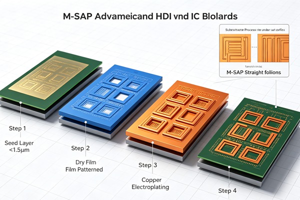
Furthermore, the demand for higher bandwidth in telecom and datacom infrastructure necessitates stringent control over trace geometry. Traditional subtractive etching results in traces with a trapezoidal cross-section. At higher frequencies, the skin effect dictates that the current travels primarily along the perimeter of the trace. The irregular edges and varying top-to-bottom widths of subtracted traces introduce impedance discontinuities, cross-talk, and significant insertion losses. Achieving sub-25 micron L/S with a precisely controlled rectangular cross-section is imperative for minimizing these parasitic effects and ensuring pristine signal transmission at multi-gigahertz frequencies.
Traditional Subtractive vs. M-SAP Processes
To fully appreciate the paradigm shift brought by M-SAP technology, one must contrast it with the conventional subtractive manufacturing method. Learn more about Return Path Optimization: Designing Solid Reference Planes for High-Frequency Signal Integrity.
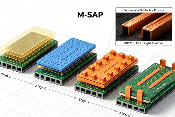
In a traditional subtractive process, a PCB starts as a laminate panel completely covered with a relatively thick layer of copper foil (typically 12 to 35 microns, equivalent to half-ounce to one-ounce copper). A photoresist is applied, exposed, and developed to protect the desired trace patterns. The unprotected copper is then chemically etched away. The primary limitation here is the isotropic nature of the etching process. The etchant removes copper not only vertically but also laterally, undercutting the photoresist. This physical constraint limits the minimum achievable line width and space to approximately 40 to 50 microns. Any attempt to push further results in compromised trace structural integrity, inconsistent impedance, or complete trace delamination.
Conversely, M-SAP begins with a very thin copper foil (usually 1.5 to 3 microns) or an ultra-thin electroless copper seed layer laminated over the dielectric base. The photoresist is applied and patterned, creating precisely defined trenches where the traces will be formed. Copper is then electrolytically plated up within these trenches. Once the plating reaches the desired thickness, the photoresist is stripped, leaving the robust plated traces alongside the exposed thin seed layer. Finally, a rapid, highly controlled “flash etch” removes the thin seed layer from the substrate. Because the seed layer is extremely thin, the flash etch takes mere seconds, minimizing any lateral attack on the plated traces. The result is straight vertical sidewalls, rectangular cross-sections, and reliable sub-25 micron L/S routing.
Key Advantages of Modified Semi-Additive Process
The adoption of M-SAP technology provides compelling engineering benefits that extend far beyond simple miniaturization, deeply impacting the electrical performance and reliability of the end product.
First and foremost is the precision of trace geometry. The additive plating process, tightly confined within LDI-defined photoresist trenches, yields exceptionally straight trace walls. This rectangular profile is vital for radio frequency (RF) and high-speed digital designs. It provides highly predictable and stable impedance characteristics, drastically reducing signal reflections, signal attenuation, and electromagnetic interference (EMI).
Secondly, M-SAP significantly increases routing density. By enabling sub-25 micron line/space, designers can route more signals within the same layer. This critical capability allows engineers to reduce the total number of layers required for a given complex schematic. This reduction in layer count can offset the higher manufacturing costs associated with the sophisticated M-SAP process, resulting in a thinner overall board profile, lighter weight, and potentially lower overall material costs.
Finally, M-SAP enhances structural reliability in ultra-fine pitch applications. The ability to plate dense structures without the risk of over-etching ensures that fine traces maintain their mechanical integrity during thermal cycling and physical stress. The strong adhesion of the plated copper to the ultra-thin seed layer provides a robust interconnect structure that resists micro-cracking and failure under demanding environmental conditions.
How to Implement M-SAP for PCB Manufacturing (Step-by-Step Guide)
Follow these engineering rules.
- Substrate Preparation and Seed Layer Deposition
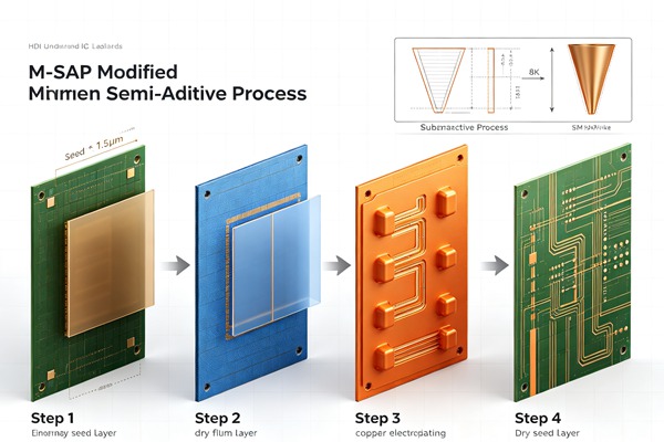
The process begins with a specialized dielectric material optimized for high-frequency performance, low dissipation factor, and minimal surface roughness. A very thin seed layer of copper is established on this dielectric. This can be achieved either by laminating ultra-thin copper foil (typically 1.5 to 3.0 μm) onto the prepreg using a carrier foil for stability, or by depositing a thin layer of electroless copper directly onto a chemically desmeared and conditioned dielectric surface. The absolute uniformity and high peel strength adhesion of this seed layer are critical prerequisites for the subsequent plating steps.
- Photoresist Application and Laser Direct Imaging (LDI)
A specialized high-resolution dry film photoresist is laminated over the delicate seed layer. To resolve ultra-fine sub-25 micron features, traditional photolithography using physical glass masks is entirely insufficient due to diffraction and alignment tolerances. Laser Direct Imaging (LDI) is strictly employed to expose the photoresist. LDI uses a highly focused laser beam to write the circuit pattern directly from CAD data onto the resist, automatically compensating for any dimensional scaling or distortion in the substrate panel in real-time. The unexposed resist is then developed away, leaving deep, perfectly vertical trenches that define the precise routing channels.
- Electrolytic Copper Plating
The panel is submerged in a highly controlled electrolytic plating bath. The thin copper seed layer acts as the cathode, conducting electrical current across the entire board surface. Copper ions from the solution are deposited selectively only into the exposed trenches where the photoresist has been removed. Advanced plating chemistries with carefully balanced organic additives—specifically levelers, brighteners, and carriers—are utilized to ensure perfectly uniform copper deposition within these micro-trenches, preventing “dog-boning” or uneven trace heights across varying pattern densities.
- Photoresist Stripping
Once the electrolytic plating has built the robust copper traces up to the desired engineering specification thickness (e.g., 12 to 20 μm), the remaining dry film photoresist must be cleanly removed. Aggressive chemical strippers are applied to dissolve and wash away the resist, exposing the newly formed rectangular traces and the original ultra-thin copper seed layer resting between them.
- Flash Etching of the Seed Layer
The final and arguably most delicate step is the differential flash etch. A highly aggressive but meticulously controlled etchant is used to rapidly dissolve the exposed thin seed layer, electrically isolating the individual copper traces. Because the seed layer is only a few microns thick, the etching process is extremely brief. This deliberate brevity minimizes the lateral etching (undercutting) of the thicker plated traces, preserving their rectangular profile, impedance characteristics, and structural integrity. Meticulous automated control of etching chemistry, temperature, and spray pressure is mandatory to ensure complete removal of the seed layer without compromising the critical sub-25 micron trace widths.
Transitioning to M-SAP technology requires specialized fabrication equipment, stringent cleanroom environmental controls, and a precise sequence of chemical and mechanical operations.
Design Considerations for M-SAP
Designing for M-SAP technology requires electrical and layout engineers to significantly update their design rules, simulation models, and material selection criteria. The most immediate impact is the relaxation of conventional trace width and spacing limitations, but working at the sub-25 micron scale introduces severe new challenges.
Surface roughness of the dielectric and the copper foil becomes a dominant factor in signal loss at frequencies above 10 GHz. Designers must specify ultra-low profile (ULP) or hyper-low profile (HLP) copper foils and premium low-loss laminate materials. The interaction between the plated copper and the specific surface finish (such as ENIG, ENEPIG, or Immersion Silver) must also be carefully modeled in 3D electromagnetic field solvers.
When routing high-speed differential pairs at sub-25 micron geometries, the coupling between the traces is intense. Maintaining exact spacing over long runs is critical for differential impedance control. The LDI process in M-SAP excels at this, providing near-perfect parallel alignment, but the design must account for tight manufacturing tolerances to avoid phase skew.
Furthermore, thermal management becomes a critical consideration. Packing dense logic and fine traces into a smaller area significantly increases the localized heat flux density. Engineers must integrate advanced thermal dissipation strategies, such as dense thermal via arrays, embedded copper coins, and high thermal conductivity dielectrics, to prevent overheating and maintain long-term reliability. The aspect ratio of the traces (height vs. width) must also be managed. While M-SAP allows for extremely narrow traces, excessively tall and narrow traces can be structurally unstable and prone to peeling during subsequent lamination cycles. Close collaboration with the PCB fabricator is essential to define an optimal stack-up and design rule check (DRC) profile.
Applications in Next-Generation Electronics
The capability to manufacture sub-25 micron L/S reliably is accelerating innovation and enabling new form factors across multiple high-tech sectors. Learn more about Sequential Lamination: Mastering the Manufacturing Process for Any-Layer HDI Boards.
In the mobile and consumer electronics space, smartphones, smartwatches, and AR/VR headsets rely heavily on M-SAP technology. It allows manufacturers to cram more sophisticated functionality—including multiple high-resolution cameras, massive on-device AI processing power, and multi-band 5G mmWave modems—into ever-shrinking, thermally constrained form factors. The HDI boards in these devices utilize Any-Layer interstitial via hole (IVH) structures deeply intertwined with ultra-fine M-SAP routing.
In the automotive industry, the rapid proliferation of autonomous driving and ADAS requires immense processing of data from radar, LiDAR, and camera sensors. The central processing modules for these systems demand extremely high-density interconnections that can operate flawlessly in harsh, high-vibration, and high-temperature environments. M-SAP provides the necessary routing density and uncompromising signal integrity for these mission-critical safety applications.
High-Performance Computing (HPC), AI accelerators, and data center infrastructure also heavily leverage M-SAP. Servers processing complex artificial intelligence workloads require immense memory bandwidth and rapid, low-latency communication between massive CPUs, parallel GPUs, and high-bandwidth memory (HBM) modules. Substrate-like PCBs (SLPs), manufactured using the M-SAP process, effectively bridge the physical gap between traditional printed circuit board technology and advanced IC packaging, enabling these critical high-speed interconnects.
Additionally, the medical device sector benefits immensely from M-SAP. Advanced implantable devices, miniaturized diagnostic equipment, and high-resolution medical imaging systems require ultra-compact electronics that maintain absolute reliability. M-SAP allows for the miniaturization of complex sensor arrays and processing units, improving patient comfort and diagnostic capabilities. Learn more about AOI & 3D X-Ray: Achieving Zero-Defect PCB Assembly.
Frequently Asked Questions (FAQ)
While both are semi-additive processes, Advanced Semi-Additive Process (ASAP) typically starts with a completely bare dielectric and uses electroless copper or sputtering to create a microscopic, ultra-thin seed layer (often less than 1 micron). This allows for even finer geometries (sub-10 micron L/S), but it is primarily used for IC substrates. M-SAP (Modified SAP) usually utilizes an ultra-thin laminated copper foil (1.5 to 3 microns) as the starting seed layer, making it more compatible with standard HDI PCB manufacturing equipment and panel sizes while still successfully achieving sub-25 micron L/S.
Initially, yes. The required fabrication equipment (such as specialized LDI machines and highly controlled plating lines), advanced thinner materials, and tighter cleanroom process controls increase the raw manufacturing costs per square inch. However, because M-SAP allows for a dramatic increase in routing density, it can often reduce the total number of layers required for a complex board design. In many dense architectures, the cost savings from a reduced layer count and smaller overall board area more than offset the premium of the M-SAP fabrication process.
M-SAP requires specific laminates with high dimensional stability, exceptionally low surface roughness, and excellent chemical adhesion properties to support the ultra-thin seed layer. While many modern high-Tg FR4 variants are compatible, demanding high-frequency designs often necessitate specialized low-loss materials (like PTFE-blends, liquid crystal polymers (LCP), or specific advanced thermoset resins) tailored specifically for the M-SAP process to minimize insertion loss and maximize signal integrity.
M-SAP drastically improves signal integrity. Traditional subtractive etching creates traces with a trapezoidal profile, which leads to impedance mismatches and higher signal loss, particularly at high frequencies due to the skin effect pushing current into the rough, etched sidewalls. M-SAP’s additive plating process creates precisely defined rectangular traces with smooth, vertical sidewalls. This results in highly consistent impedance, lower insertion loss, and vastly superior high-speed signal transmission capabilities.
The primary challenge in flash etching is achieving uniform removal of the thin seed layer across the entire large production panel without aggressively attacking the sidewalls of the newly plated copper traces. This requires maintaining extremely tight control over the etchant bath chemistry, precise temperature regulation, and optimized spray nozzle configurations. Any over-etching will undercut the traces, ruining their rectangular profile and compromising the sub-25 micron line width tolerance.