Table of Contents
The Challenge of Multi-Gigabit Routing in Modern Hardware
We have officially entered an era where digital design is inherently analog. With the adoption of multi-gigabit interfaces like PCIe 5.0 (32 GT/s) and DDR5 (up to 8400 MT/s), signals no longer behave like simple binary states. Instead, they propagate as complex electromagnetic waves, making them exquisitely sensitive to the physical geometry of your printed circuit board.
At these extreme frequencies, every via, every bend in a trace, and every slight variation in dielectric thickness acts as a potential point of signal degradation. In this technical deep dive, we will explore the high speed PCB routing techniques required to maintain signal integrity (SI), preserve an open eye diagram, and ensure your cutting-edge designs boot up perfectly on the first spin.
The Three Pillars of Signal Integrity
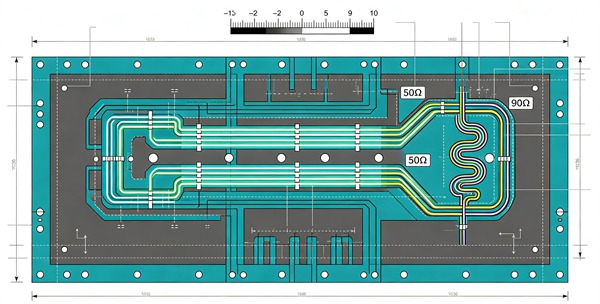
Before laying down a single trace, high-speed routing demands a flawless foundation. Signal integrity at multi-gigabit speeds relies on three primary pillars: Impedance Control, Loss Minimization, and Crosstalk Mitigation.
Strict Impedance Control
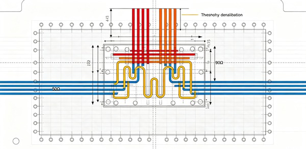
For PCIe 5.0, differential impedance is typically targeted at 85 ohms (±10%), while DDR5 single-ended signals target 40-50 ohms depending on the specific JEDEC standard. Impedance is dictated by trace width, trace spacing, and the distance to the reference plane. Even minor manufacturing deviations—such as over-etching the copper—can cause impedance mismatches, leading to signal reflections (return loss).
Dielectric and Copper Losses
At 16 GHz (the Nyquist frequency of PCIe 5.0), the loss tangent (Df) of your PCB material absorbs a significant amount of the signal energy, turning it into heat. Furthermore, the “skin effect” forces high-frequency currents to travel only on the outermost microns of the copper trace. Rough copper surfaces dramatically increase this resistance, severely attenuating the signal over distance.
Crosstalk and Return Paths
When high-speed traces run parallel for too long, electromagnetic coupling induces noise (crosstalk) into adjacent lines. Equally important is the return path: high-frequency signals will always take the path of least inductance, which is directly underneath the trace on the nearest reference plane. If that plane is broken by a split or a void, the signal will radiate Electromagnetic Interference (EMI) and degrade significantly.
How to Route High Speed Signals (Step-by-Step Guidelines)
Follow these engineering rules.
- Secure an Unbroken Reference Plane
Never route a high-speed signal across a split in the ground or power plane. The trace must have a continuous, unbroken reference plane directly beneath it for its entire length to maintain a tight return current loop. If a signal must change layers, ensure a ground transfer via (stitching via) is placed right next to the signal via to provide a continuous return path.
- Optimize Differential Pairs
Route differential pairs tightly coupled and perfectly symmetrical. If an obstacle (like a via or a component) forces the pair to separate, bring them back together as quickly as possible. Maintain phase matching (length matching within the pair) to a tolerance of less than 5 mils. Any length mismatch translates to timing skew, which converts differential signals into common-mode noise.
- Choose Between Microstrip and Stripline
Microstrip (Surface Layers): Faster propagation speed, but higher radiation and crosstalk susceptibility. Suitable for shorter runs.
Stripline (Internal Layers): The trace is sandwiched between two ground/power planes. Offers excellent EMI shielding and lower crosstalk. For multi-gigabit signals like PCIe 5.0, internal stripline routing is highly recommended. - Implement the 3W/5W Rule
To mitigate crosstalk, maintain a distance of at least 3 times the trace width (3W) between adjacent high-speed single-ended traces. For critical differential pairs like PCIe 5.0, aim for 5W spacing to neighboring signals to prevent near-end and far-end crosstalk (NEXT and FEXT).
- Avoid 90-Degree Bends
Sharp corners create an abrupt change in trace capacitance, causing impedance discontinuities. Use smooth arcs or 45-degree chamfered bends for all high-speed routing.
- Manage Via Stubs via Backdrilling
When a signal transitions from layer 1 to layer 3 on a 10-layer board, the remaining copper barrel from layer 3 to layer 10 acts as an antenna. This creates a resonant stub that utterly destroys multi-gigabit signals by creating deep notches in the frequency response. You must specify backdrilling (controlled depth drilling) to physically remove these unused via stubs. Alternatively, leverage [Any Layer HDI PCB Manufacturing](/mastering-any-layer-hdi-pcb-manufacturing) to use blind microvias and avoid stubs altogether.
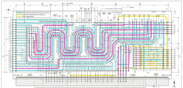
Implementing advanced high speed PCB routing techniques requires strict adherence to physical design rules. Apply the following steps when routing memory or high-speed serial interfaces.
Material Selection for PCIe 5.0 and DDR5
Standard FR4 is dead at 32 GT/s. You cannot fix with routing what is broken by physics. For PCIe 5.0 and DDR5, you must upgrade your PCB substrate.
- Ultra-Low Loss Laminates: Specify materials like Panasonic Megtron 6, Megtron 7, or Rogers high-frequency laminates. These materials offer an ultra-low loss tangent (Df < 0.004) and a highly stable dielectric constant across wide frequency bands.
- Ultra-Low Profile (ULP) Copper: To combat the skin effect, specify perfectly smooth copper foils (often called HVLP – Hyper Very Low Profile). Rough copper acts like microscopic speed bumps for high-frequency signals.
If your design also demands dynamic mechanical flexibility, ensuring signal integrity becomes even more complex. Review our insights on Navigating Rigid Flex PCB Design Rules to understand how polyimide affects impedance.
Understanding the Eye Diagram
When evaluating high-speed SI, engineers look at the “Eye Diagram.” An open eye indicates a healthy signal with clear differentiation between 1s and 0s and plenty of timing margin. A “closed eye” means jitter and attenuation have destroyed the signal. Applying the techniques above—specifically minimizing loss and crosstalk—is the only way to keep the eye open at PCIe 5.0 speeds.
Frequently Asked Questions (FAQ)
DDR5 operates at much higher data rates and utilizes a different architecture, featuring two independent 32-bit channels per DIMM. It requires much tighter length matching, stricter impedance control, and highly optimized power delivery networks (PDN) right on the motherboard to support its on-die PMIC.
Without active signal conditioning (like retimers or redrivers), PCIe 5.0 signals are incredibly loss-limited. Depending on your PCB material, the absolute maximum trace length before the signal degrades beyond recovery is typically between 5 to 8 inches.
Yes. Teardrops add a smooth transition of copper from the trace to the via pad. This reduces the risk of drill breakout during manufacturing and prevents a sudden impedance discontinuity at the via junction.
Conclusion
As we push into the realm of PCIe 5.0 and DDR5, the margin for error in PCB design has vanished. Mastering high speed PCB routing techniques is no longer optional—it is a mandatory prerequisite for modern electronics. By enforcing strict impedance control, utilizing ultra-low loss materials, eliminating via stubs, and ruthlessly protecting return paths, you can ensure your hardware achieves maximum bandwidth without falling victim to signal degradation.