Table of Contents
The Evolution of Electronic Packaging
Early electronic products mainly used Dual In-line Package (DIP) components. DIP packages were easy to assemble and repair, but occupied large PCB space and supported limited pin counts.
As integrated circuits became more complex, Quad Flat Package (QFP) technology emerged. QFP increased pin density by placing leads around all four sides of the package. However, when pin counts exceeded several hundred, lead pitch became extremely fine, increasing the risks of bridging, coplanarity issues, and signal integrity problems.
BGA technology solved many of these limitations by replacing peripheral leads with solder balls distributed across the bottom of the package.
Instead of relying on fragile external leads, BGA uses an array of solder balls to connect directly to the PCB. This design dramatically increases connection density while improving thermal and electrical performance.
For high-speed and high-power devices, BGA has become the industry standard.
You can also learn more about advanced PCB structures in our related guide on multilayer PCB manufacturing and high-density interconnect design.
What Is a BGA Package?
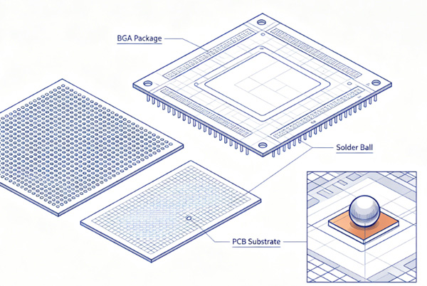
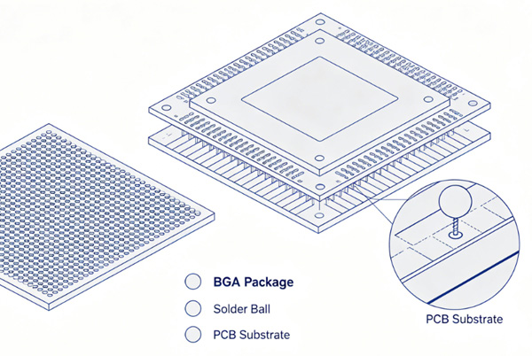
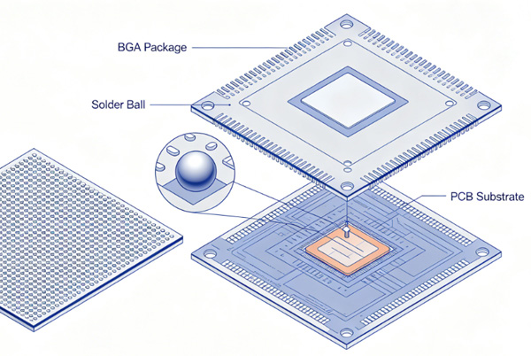
Ball Grid Array (BGA) is a surface-mount packaging technology that uses solder balls arranged in a grid pattern underneath the package to create electrical and mechanical connections with the PCB.
Unlike QFP packages, where pins extend outward from the package edges, BGA packages place connections underneath the component body.
This approach offers several advantages:
- Higher pin count capability
- Smaller package footprint
- Better heat dissipation
- Reduced signal inductance
- Improved electrical reliability
BGA technology is especially suitable for:
- High-speed processors
- FPGA devices
- Memory modules
- RF communication chips
- AI accelerators
- Automotive ECUs
Basic Structure and Working Principle of BGA
A BGA package typically consists of several major elements.
Substrate
The substrate acts as the carrier between the silicon die and the PCB. It routes signals from the chip to the solder balls underneath.
The substrate may be used:
- BT resin
- Ceramic materials
- High-frequency laminates
- Multi-layer organic substrates
Advanced packages often include microvias and fine-trace routing, similar to HDI PCB structures.
Bond Pads
Bond pads provide electrical connections between the silicon die and the substrate routing layers.
Depending on the package type, connections may use:
- Wire bonding
- Flip-chip interconnection
- Copper pillar technology
Solder Balls
Solder balls are the defining feature of BGA packaging.
These solder spheres serve two purposes:
- Electrical interconnection
- Mechanical attachment
Lead-free solder alloys such as SAC305 are commonly used in modern manufacturing.
Encapsulation Materials
Molding compounds protect the die and internal interconnections from:
- Moisture
- Mechanical stress
- Contamination
- Thermal cycling damage
Some high-power BGAs also include integrated heat spreaders or thermal lids.
How BGA Works
During SMT assembly, solder paste is printed onto the PCB pads. The BGA component is then placed onto the board using pick-and-place equipment.
During reflow soldering:
- Solder paste melts
- Solder balls collapse
- Surface tension aligns the package automatically
- Electrical and mechanical joints form simultaneously
This self-alignment effect is one reason why BGA packages can achieve highly accurate placement despite having hundreds or thousands of connections.
Main Types of BGA Packages
Different applications require different BGA structures.
Plastic BGA (PBGA)
PBGA uses organic laminate substrates and plastic encapsulation materials.
Advantages:
- Lower manufacturing cost
- Good electrical performance
- Widely used in consumer electronics
Applications include:
- GPUs
- Memory devices
- Consumer processors
Ceramic BGA (CBGA)
CBGA uses ceramic substrates instead of organic materials.
Advantages:
- Excellent thermal stability
- Better reliability under harsh environments
- Lower thermal expansion mismatch
Commonly used in:
- Aerospace electronics
- Military systems
- Industrial control equipment
Heat Sink BGA (HSBGA)
HSBGA integrates thermal structures for improved heat dissipation.
These packages are commonly found in:
- High-performance processors
- AI accelerators
- Networking equipment
Micro BGA (µBGA / CSP)
Micro BGA and Chip Scale Package (CSP) technologies focus on miniaturization.
Features include:
- Extremely small footprint
- Fine pitch interconnection
- Lightweight structure
Widely used in:
- Smartphones
- Wearable devices
- Compact IoT modules
Flip-Chip BGA (FCBGA)
FCBGA directly connects the die to the substrate using solder bumps.
Advantages:
- Very short signal path
- Excellent electrical performance
- Superior thermal capability
FCBGA is commonly used for:
- CPUs
- GPUs
- High-speed networking chips
- AI computing processors
Key Advantages of BGA Technology
Higher I/O Density
BGA packages can support significantly more connections than QFP packages of similar size.
This enables complex devices with:
- High data bandwidth
- Multi-core architectures
- Large memory interfaces
Better Thermal Performance
The bottom solder ball structure improves heat transfer to the PCB.
Additional thermal vias and copper planes can further improve cooling efficiency.
For thermal management design, PCB stackup planning also plays a critical role.
Improved Electrical Performance
BGA reduces:
- Lead inductance
- Signal reflection
- EMI issues
Shorter electrical paths make BGA highly suitable for:
- DDR memory
- PCIe systems
- RF circuits
- High-speed digital interfaces
Self-Alignment During Reflow
Surface tension naturally centers the package during solder reflow.
This improves assembly accuracy and reduces sensitivity to placement tolerances.
Support for High-Frequency Designs
Modern high-speed systems require controlled impedance and low parasitic effects.
BGA structures help maintain signal integrity in advanced electronic systems.
BGA Manufacturing and Assembly Process
Successful BGA assembly depends heavily on process control.
Substrate Manufacturing
The substrate is fabricated using multi-layer PCB manufacturing techniques, including:
- Laser drilling
- Fine-line etching
- Sequential lamination
- Microvia formation
Solder Ball Attachment
Common solder ball attachment methods include:
- Ball placement machines
- Flux-assisted ball mounting
- Stencil printing processes
Ball diameter and pitch must be tightly controlled.
Solder Paste Printing
Accurate solder paste deposition is critical for avoiding defects such as:
- Bridging
- Insufficient solder
- Head-in-pillow defects
Stencil thickness and aperture design significantly affect yield rates.
Reflow Soldering
The reflow profile must be optimized for:
- Peak temperature
- Ramp rate
- Soak duration
- Cooling rate
Improper thermal profiles may cause solder fatigue or voiding.
Underfill Process
Some applications require underfill materials between the BGA and PCB.
Underfill improves:
- Mechanical strength
- Thermal cycling reliability
- Vibration resistance
It is commonly used in automotive and mobile electronics.
BGA Inspection and Rework Challenges
One major challenge of BGA technology is that solder joints are hidden underneath the package.
Traditional visual inspection methods are insufficient.
X-Ray Inspection
X-ray systems are the most common BGA inspection solution.
They detect:
- Voids
- Bridging
- Missing solder balls
- Alignment problems
Modern SMT factories often use both 2D and 3D X-ray systems.
Electrical Testing
Functional testing and in-circuit testing help verify electrical continuity.
Boundary scan testing is also widely used for complex BGA devices.
Optical and Laser Inspection
Advanced systems can evaluate package coplanarity and placement accuracy before reflow.
BGA Rework Process
Reworking BGA packages requires specialized equipment and operator experience.
- Step 1: BGA Removal
The defective component is heated using controlled top and bottom heaters until the solder melts.
The package is then removed carefully to avoid PCB pad damage. - Step 2: Pad Cleaning
Residual solder is cleaned using solder wick and flux.
Pads must remain flat and uncontaminated. - Step 3: Reballing
New solder balls are attached using reballing stencils.
Accurate ball alignment is essential. - Step 4: Reinstallation and Reflow
The repaired BGA is placed back onto the PCB and reflowed again.
Temperature profiles must be carefully controlled to avoid warpage.
Common BGA Defects and Solutions
Bridging
Excess solder may create unintended electrical connections.
Common causes:
- Excess solder paste
- Misalignment
- Poor stencil design
Cold Solder Joints and Head-in-Pillow
Incomplete wetting may create unreliable electrical connections.
Solutions include:
- Optimized reflow profiles
- Improved flux activity
- Better coplanarity control
Voids
Gas trapped inside solder joints creates voids.
Excessive voiding can reduce thermal conductivity and reliability.
Solder Ball Loss
Improper handling or moisture exposure may cause solder balls to detach.
MSL (Moisture Sensitivity Level) control is critical.
Solder Joint Cracking
Thermal cycling and mechanical stress can cause fatigue cracks over time.
Solutions include:
- Underfill materials
- Improved PCB support
- Optimized solder alloys
Applications of BGA Packages
Computing and Servers
BGA packages are widely used in:
- CPUs
- GPUs
- Chipsets
- High-speed memory
Mobile Devices
Smartphones and tablets rely heavily on compact BGA and CSP technologies.
Communication Equipment
RF modules and baseband processors require high-speed interconnections and low signal loss.
Automotive Electronics
Automotive ECUs, ADAS systems, and sensor modules increasingly depend on BGA reliability.
AI and Data Center Hardware
AI accelerators generate enormous power density and require advanced thermal packaging solutions such as FCBGA and HSBGA.
Future Trends of BGA Technology
Smaller Pitch Sizes
BGA pitch continues to shrink below 0.3 mm to support higher-density devices.
Integrated Thermal Structures
Future packages increasingly integrate:
- Molded heat spreaders
- Vapor chambers
- Advanced thermal interface materials
Heterogeneous Integration
Modern systems combine multiple chip types within a single package.
This includes:
- CPU + GPU integration
- Memory stacking
- RF integration
Synergy With SiP, 3D Packaging, and Chiplet Architectures
BGA technology continues evolving alongside:
- System-in-Package (SiP)
- 2.5D packaging
- 3D IC integration
- Chiplet architectures
These technologies are reshaping next-generation computing systems.
Conclusion
BGA technology has become one of the most important packaging solutions in modern electronics manufacturing.
Its ability to support high pin counts, compact layouts, high-speed signaling, and efficient thermal management makes it essential for advanced electronic products.
However, successful BGA manufacturing requires:
- Precise PCB design
- Controlled SMT assembly
- Advanced inspection capability
- Skilled rework processes
As semiconductor integration continues to increase, BGA and related advanced packaging technologies will remain critical to future electronics development.
FAQ
A: BGA stands for Ball Grid Array. It is a surface-mount package that uses solder balls underneath the package for PCB connection.
A: BGA provides higher pin density, better thermal performance, shorter signal paths, and improved electrical characteristics compared with QFP packages.
A: Yes. BGA packages can be reworked using specialized rework stations, X-ray inspection systems, and reballing equipment.
A: Because the solder joints are hidden underneath the package, visual inspection cannot accurately evaluate solder quality.