PCB stackup design is one of the most important stages in circuit board development. A well-designed stackup improves signal integrity, power distribution, electromagnetic compatibility (EMC), thermal performance, and overall manufacturing reliability.
Many PCB issues that appear during testing are not caused by schematic errors or component selection, but by poor layer arrangement and inadequate stackup planning.
Whether you are designing a simple four-layer board or a complex high-speed communication system, understanding stackup design principles can help improve performance and reduce manufacturing risks.

Table of Contents
What Is a PCB Stackup?
A PCB stackup refers to the arrangement of copper layers and dielectric materials that form a multilayer printed circuit board.
The stackup defines:
- Signal layer placement
- Power plane structure
- Ground plane configuration
- Material thickness
- Copper thickness
- Controlled impedance parameters
The layer structure directly influences electrical performance and manufacturability.
A stackup should always be planned before routing begins because trace widths, spacing, impedance values, and return current paths depend on the layer arrangement.
Why PCB Stackup Design Matters
A properly designed stackup provides several important benefits.
Improved Signal Integrity
High-speed signals require stable reference planes and controlled impedance.
Proper layer planning helps reduce:
- Signal reflections
- Crosstalk
- Timing errors
- Data corruption
Better EMI Performance
Electromagnetic interference becomes increasingly important in modern electronic products.
A balanced stackup helps:
- Minimize radiation
- Reduce susceptibility to external noise
- Improve EMC compliance
Stable Power Distribution
Power integrity is often overlooked during PCB design.
Proper plane structures help:
- Reduce voltage fluctuations
- Lower power noise
- Improve system stability
Easier Manufacturing
A well-balanced stackup improves:
- Lamination stability
- Registration accuracy
- Yield rates
- Overall production consistency
Related service: Multilayer PCB Manufacturing
Basic Components of a PCB Stackup
Signal Layers
Signal layers carry digital, analog, RF, and power routing traces.
These layers should be positioned close to solid reference planes whenever possible.
Ground Planes
Ground planes provide return current paths and shielding.
Continuous ground planes are one of the most effective methods for improving signal integrity.
Benefits include:
- Reduced EMI
- Lower impedance return paths
- Better noise control
Power Planes
Power planes distribute voltage throughout the PCB.
Dedicated power layers help reduce voltage drop and improve power delivery.
Dielectric Layers
Dielectric materials separate copper layers.
Their characteristics influence:
- Impedance
- Signal propagation speed
- Electrical isolation
- PCB thickness
Material selection becomes especially important for high-speed and RF applications.
Related article: High-Frequency PCB Manufacturing
Common PCB Stackup Configurations
2-Layer PCB Stackup
Typical structure:
- Top Signal
- Bottom Signal
Common applications:
- Consumer electronics
- LED products
- Simple control circuits
Advantages:
- Low cost
- Simple manufacturing
Limitations:
- Poor EMI control
- Limited routing space
4-Layer PCB Stackup
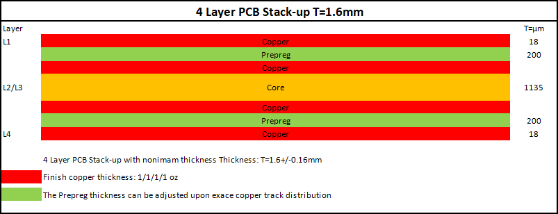
A common configuration:
| Layer | Function |
|---|---|
| L1 | Signal |
| L2 | Ground Plane |
| L3 | Power Plane |
| L4 | Signal |
Advantages:
- Improved signal integrity
- Better EMI performance
- Easier impedance control
This is often the preferred starting point for industrial electronics.
6-Layer PCB Stackup
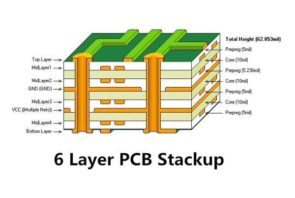
A typical example:
| Layer | Function |
|---|---|
| L1 | Signal |
| L2 | Ground |
| L3 | Signal |
| L4 | Signal |
| L5 | Power |
| L6 | Signal |
Benefits include:
- Higher routing density
- Better isolation
- Improved EMC performance
8-Layer and Higher Stackups
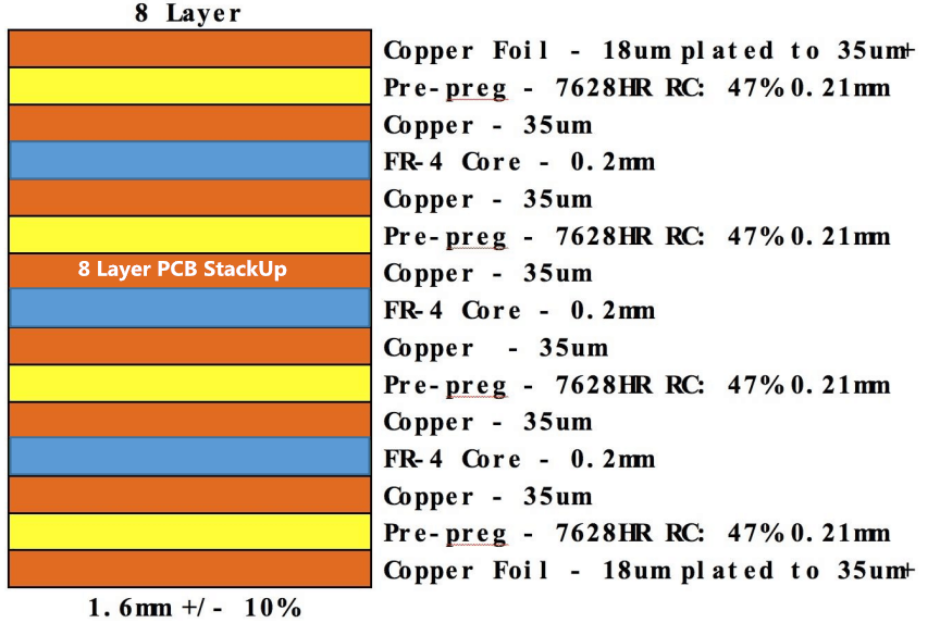
Advanced applications frequently use:
- 8-layer PCBs
- 10-layer PCBs
- 12-layer PCBs
- 16-layer PCBs and above
These structures support:
- High-speed processors
- Networking equipment
- AI hardware
- Communication systems
- Aerospace electronics
PCB Stackup Design Principles
Keep Ground Planes Continuous
Ground plane interruptions force return currents to find alternative paths.
This may increase:
- EMI
- Signal distortion
- Crosstalk
Continuous reference planes are generally preferred.
Place Signal Layers Adjacent to Reference Planes
Every high-speed signal should have a nearby reference plane.
Benefits include:
- Stable impedance
- Reduced emissions
- Better signal quality
Maintain Stackup Symmetry
Symmetrical stackups help reduce board warpage during manufacturing.
Balanced copper distribution also improves lamination stability.
Separate High-Speed and Noisy Signals
Sensitive circuits should be isolated from:
- Switching power supplies
- Motor drivers
- High-current traces
- RF transmitters
Proper layer assignment helps reduce interference.
Controlled Impedance and Stackup Design
Modern communication interfaces often require controlled impedance routing.
Common targets include:
| Signal Type | Typical Impedance |
|---|---|
| Single-ended RF | 50Ω |
| Ethernet Differential Pair | 100Ω |
| USB Differential Pair | 90Ω |
| LVDS Differential Pair | 100Ω |
Impedance depends on:
- Trace width
- Copper thickness
- Dielectric thickness
- Material dielectric constant
- Layer arrangement
Manufacturers usually calculate impedance values based on the approved stackup before production begins.
Stackup Design for High-Speed PCBs
As data rates increase, stackup quality becomes increasingly important.
Design considerations include:
Return Current Paths
High-speed signals always require low-impedance return paths.
Poor return path design often causes signal integrity issues.
Layer Transition Management
Every via introduces electrical discontinuities.
Designers should minimize unnecessary layer transitions where possible.
Differential Pair Routing
Differential signals require:
- Consistent spacing
- Length matching
- Stable reference planes
These factors should be considered during stackup planning.
Material Selection for PCB Stackups
Standard FR4
Suitable for:
- Industrial electronics
- Consumer products
- General-purpose designs
Advantages:
- Cost-effective
- Readily available
- Easy to manufacture
Low-Loss Materials
Applications requiring higher frequencies may use:
- Rogers materials
- Panasonic laminates
- Isola high-speed materials
Benefits include:
- Reduced insertion loss
- Better signal quality
- Improved high-frequency performance
Thermal Considerations in Stackup Design
Heat management should be addressed early in the design process.
Stackup choices affect:
- Heat spreading
- Thermal resistance
- Power distribution
Techniques include:
- Thick copper layers
- Thermal vias
- Dedicated copper planes
- Metal-core structures
Related service: Metal Core PCB
Manufacturing Considerations
A stackup that looks acceptable in CAD software may still create manufacturing challenges.
Engineers should consider:
Copper Balance
Uneven copper distribution can cause:
- Warpage
- Lamination issues
- Registration problems
Standard Material Availability
Using standard prepreg and core thicknesses often reduces manufacturing cost and lead time.
Drill Aspect Ratio
Stackup thickness directly affects drilling capability.
Excessive aspect ratios may reduce manufacturing yield.
Layer Registration
Higher layer counts require tighter alignment control.
Manufacturers should review stackups during DFM analysis to ensure manufacturability.
Related reading: How to Find a PCB Manufacturer With Quick Turnaround
Common Stackup Design Mistakes
Some of the most frequent issues include:
- Missing ground planes
- Poor layer symmetry
- Excessive layer transitions
- Incorrect impedance calculations
- Mixed signal and power routing
- Inadequate isolation between noisy and sensitive circuits
Many of these problems can be avoided through early collaboration with the PCB manufacturer.
Working With Your PCB Manufacturer
Stackup design should not be completed in isolation.
An experienced PCB manufacturer can assist with:
- Material recommendations
- Impedance calculations
- Layer structure optimization
- DFM review
- Manufacturing capability verification
Early communication often reduces redesign cycles and shortens development schedules.
Conclusion
PCB stackup design forms the foundation of signal integrity, power integrity, EMC performance, and manufacturing reliability.
Whether designing a four-layer industrial controller or a sixteen-layer high-speed communication platform, proper stackup planning helps reduce risk and improve overall product performance.
By considering layer arrangement, impedance control, material selection, thermal management, and manufacturing requirements from the beginning of the project, engineers can achieve more reliable and cost-effective PCB designs.
FAQ
A: A PCB stackup is the arrangement of copper layers and dielectric materials that form a multilayer circuit board.
A: Stackup design affects signal integrity, impedance control, EMI performance, power distribution, thermal management, and manufacturability.
A: Four-layer and six-layer configurations are among the most commonly used stackups for industrial and commercial electronics.
A: Trace geometry, dielectric thickness, material properties, and layer arrangement all influence controlled impedance values.
A: The stackup should be defined before PCB routing begins because signal integrity and impedance calculations depend on the approved layer structure.