As signal speeds continue to increase in modern electronic devices, PCB impedance control has become a critical part of circuit board design and manufacturing. High-speed digital interfaces, RF circuits, automotive electronics, telecommunications equipment, and data center hardware all depend on stable impedance to ensure reliable signal transmission.
Without proper impedance control, signals can experience reflections, attenuation, timing errors, and electromagnetic interference, leading to reduced system performance or complete communication failure.
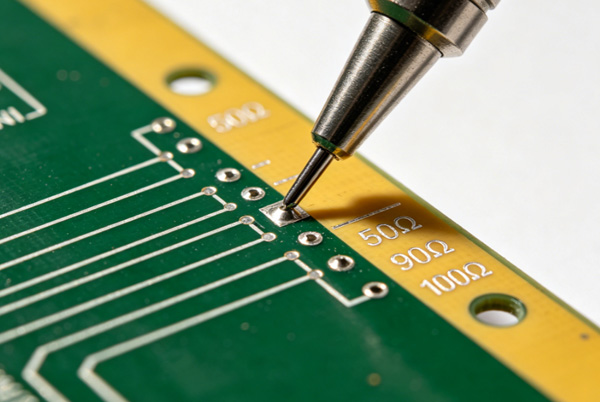
Table of Contents
What Is PCB Impedance Control?
Controlled impedance refers to the process of designing PCB traces so that they maintain a specific electrical impedance value throughout the signal path.
Impedance is determined by the interaction between:
- Trace width
- Trace thickness
- Dielectric thickness
- Dielectric constant (Dk)
- Reference plane location
- PCB stackup structure
When these variables are carefully controlled, signals can travel through the PCB with minimal distortion and predictable electrical behavior.
Controlled impedance is especially important for high-frequency and high-speed applications where signal integrity directly affects system performance.
Related article: PCB Stackup Design Guide
Why Controlled Impedance Matters
As signal frequencies increase, PCB traces no longer behave like simple electrical connections.
Instead, they function as transmission lines.
If the impedance of a trace changes unexpectedly, part of the signal energy is reflected toward the source.
These reflections may cause:
- Data corruption
- Increased jitter
- Timing violations
- Communication errors
- Reduced signal quality
Controlled impedance helps maintain signal consistency and improve overall system reliability.
Common Applications Requiring Controlled Impedance
Many modern electronic products require impedance-controlled PCBs.
Typical applications include:
High-Speed Digital Systems
Examples include:
- DDR memory
- PCIe
- USB
- HDMI
- DisplayPort
- Ethernet
RF and Microwave Circuits
RF designs often require precise impedance matching to maximize signal transmission efficiency.
Applications include:
- Antenna modules
- RF amplifiers
- Wireless communication systems
- Satellite equipment
Related article: High-Frequency PCB Manufacturing
Telecommunications Equipment
Modern networking equipment relies heavily on controlled impedance routing to maintain high data transmission rates.
Automotive Electronics
Advanced driver assistance systems (ADAS), radar modules, and vehicle communication networks frequently require impedance-controlled PCBs.
Related application: Autonomous Delivery Vehicle PCB
Types of PCB Controlled Impedance
Single-Ended Impedance
Single-ended signals use one conductor and a reference plane.
The most common target is:
- 50Ω
Single-ended impedance is widely used in RF circuits and many digital applications.
Differential Impedance
Differential signals use two traces carrying equal and opposite signals.
Common differential impedance values include:
| Interface | Typical Differential Impedance |
|---|---|
| USB | 90Ω |
| Ethernet | 100Ω |
| LVDS | 100Ω |
| PCIe | 85Ω |
| CAN Bus | 120Ω |
Differential routing improves noise immunity and supports higher data rates.
Factors That Affect PCB Impedance
Trace Width
Trace width is one of the most important variables affecting impedance.
Generally:
- Wider traces decrease impedance
- Narrower traces increase impedance
Even small dimensional variations can influence impedance performance.
Dielectric Thickness
The distance between the signal trace and the reference plane significantly affects impedance.
Increasing dielectric thickness typically increases impedance.
Dielectric Constant (Dk)
The dielectric constant of the PCB material determines how electromagnetic fields propagate through the substrate.
Materials with stable Dk values provide more predictable impedance performance.
Copper Thickness
Copper thickness influences the effective geometry of the conductor.
Manufacturing calculations must account for copper plating growth during fabrication.
PCB Stackup Structure
The stackup determines the relationship between signal layers and reference planes.
Impedance calculations cannot be finalized until the stackup has been defined.
Related article: Multilayer PCB Manufacturing
Common Controlled Impedance Structures
Microstrip
Microstrip traces are located on an outer PCB layer with a reference plane underneath.
Advantages include:
- Simple construction
- Easy manufacturing
- Lower cost
Microstrip structures are commonly used in RF designs.
Stripline
Stripline traces are embedded between reference planes.
Benefits include:
- Better shielding
- Reduced EMI
- Improved signal integrity
Stripline structures are often used in high-speed digital systems.
Differential Pair Structures
Differential pairs can be implemented as:
- Differential microstrip
- Differential stripline
Proper spacing and routing consistency are critical for maintaining differential impedance.
PCB Stackup and Impedance Planning
Controlled impedance should be considered during the earliest stages of PCB design.
A typical impedance-controlled stackup includes:
- Dedicated ground planes
- Stable dielectric layers
- Controlled trace geometries
- Balanced layer structures
Manufacturers often recommend specific stackups based on:
- Layer count
- Material selection
- Target impedance values
- Manufacturing capabilities
The final stackup should always be approved before routing begins.
Material Selection for Impedance Control
Standard FR4
FR4 is suitable for many impedance-controlled designs operating at moderate frequencies.
Advantages include:
- Cost-effectiveness
- Wide availability
- Mature manufacturing processes
Low-Loss High-Speed Materials
For advanced applications, designers may select:
- Rogers materials
- Isola laminates
- Panasonic materials
- Megtron series laminates
Benefits include:
- Lower signal loss
- Improved high-frequency performance
- Better impedance stability
These materials are frequently used in networking and RF applications.
Manufacturing Tolerances and Impedance Accuracy
Achieving controlled impedance requires strict process control.
Important manufacturing variables include:
- Trace width tolerance
- Copper thickness variation
- Material consistency
- Layer registration accuracy
- Lamination control
Typical impedance tolerance targets are:
| Application | Typical Tolerance |
|---|---|
| Standard Digital | ±10% |
| High-Speed Digital | ±8% |
| Networking Equipment | ±5% |
| RF Applications | ±5% or tighter |
Tighter tolerances generally increase manufacturing complexity and cost.
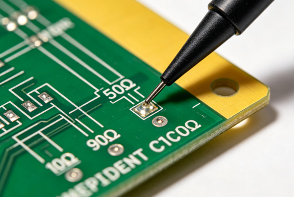
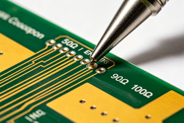
Impedance Testing Methods
Verification is a critical part of impedance-controlled PCB manufacturing.
TDR Testing
Time Domain Reflectometry (TDR) is the most common testing method.
TDR measures:
- Actual impedance values
- Impedance discontinuities
- Signal reflections
Manufacturers typically include test coupons on production panels for measurement.
Test Coupons
Impedance coupons are fabricated alongside production boards.
They provide a reliable way to verify whether manufacturing results meet design requirements.
Many OEM customers require impedance reports with shipment documentation.
Common Impedance Control Challenges
Incorrect Stackup Selection
Changing stackup parameters after routing often requires redesign.
Inaccurate Material Data
Using generic Dk values instead of manufacturer-certified material data can create impedance deviations.
Poor Differential Pair Routing
Inconsistent spacing and trace geometry may cause impedance imbalance.
Insufficient Communication With the PCB Manufacturer
Many impedance issues occur when design assumptions differ from actual manufacturing capabilities.
Early stackup review with the PCB fabricator helps avoid costly redesigns.
Design Tips for Better Impedance Control
Experienced PCB designers often follow several best practices:
- Finalize stackup before routing
- Use manufacturer-approved impedance tables
- Keep reference planes continuous
- Avoid unnecessary layer transitions
- Maintain differential pair spacing
- Minimize signal path discontinuities
- Verify calculations with simulation tools
These practices improve first-pass manufacturing success rates.
Working With a PCB Manufacturer
Successful impedance-controlled PCB projects require collaboration between design engineers and fabrication teams.
An experienced manufacturer should provide:
- Stackup recommendations
- Impedance calculations
- Material guidance
- DFM review
- Impedance testing reports
Choosing a supplier with proven impedance control capability helps reduce production risks and improve product reliability.
Related reading: What Quality Standards Indicate a Reliable PCB Manufacturer?
Conclusion
PCB impedance control is a fundamental requirement for high-speed digital circuits, RF systems, telecommunications equipment, automotive electronics, and many other advanced applications.
Achieving reliable impedance performance requires careful attention to stackup design, material selection, trace geometry, manufacturing tolerances, and testing procedures.
By integrating impedance considerations early in the design process and working closely with an experienced PCB manufacturer, engineers can improve signal integrity, reduce communication errors, and ensure long-term product performance.
FAQ
A: Controlled impedance is the practice of designing PCB traces to maintain a specific impedance value for reliable signal transmission.
A: 50Ω provides a practical balance between power handling and signal performance, making it a common standard for RF systems.
A: Single-ended impedance measures one trace relative to a reference plane, while differential impedance measures the impedance between two coupled traces.
A: Most manufacturers use TDR testing and impedance test coupons to verify that production boards meet specified impedance requirements.
A: Yes. Controlled impedance requires additional engineering, process control, testing, and tighter manufacturing tolerances, which can increase production costs.