As electronic systems continue to evolve, conventional circuit boards are no longer sufficient for many applications. High-speed data transmission, miniaturization, increased power density, and harsh operating environments have driven the development of advanced PCB technologies.
From telecommunications and automotive electronics to aerospace, medical equipment, and industrial automation, advanced PCB solutions help engineers overcome challenges related to signal integrity, thermal management, reliability, and space limitations.
Choosing the right PCB technology at the early stages of product development can significantly improve system performance and long-term reliability.
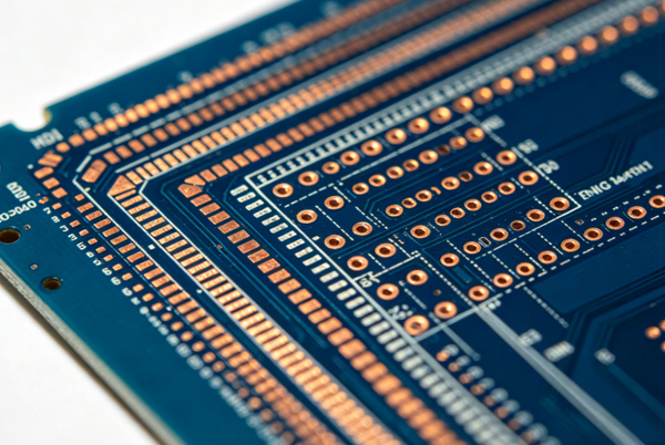
Table of Contents
What Are Advanced PCB Solutions?
Advanced PCB solutions refer to circuit board technologies that go beyond standard two-layer and four-layer FR4 designs.
These solutions are typically used when products require:
- Higher circuit density
- Better signal integrity
- Improved thermal performance
- Higher current capability
- Reduced size and weight
- Greater reliability
Advanced PCB technologies often involve specialized materials, tighter manufacturing tolerances, and more sophisticated fabrication processes.
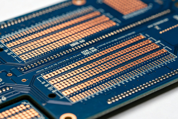
Multilayer PCB Technology
Multilayer PCBs are among the most widely used advanced PCB structures.
Typical layer counts include:
- 6-layer PCB
- 8-layer PCB
- 10-layer PCB
- 12-layer PCB
- 16-layer PCB and above
Multilayer designs provide:
- Increased routing density
- Improved signal isolation
- Better power distribution
- Enhanced EMI performance
These structures are commonly found in:
- Networking equipment
- Servers
- Industrial control systems
- Medical devices
- Communication hardware
Related service: Multilayer PCB Manufacturing
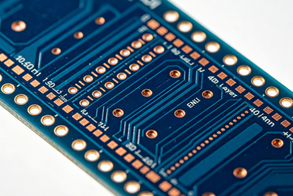
HDI PCB Solutions
High-Density Interconnect (HDI) technology enables higher circuit density within compact spaces.
HDI boards typically incorporate:
- Microvias
- Blind vias
- Buried vias
- Sequential lamination
- Fine-pitch routing
Advantages include:
- Smaller board size
- Reduced signal path length
- Better electrical performance
- Support for high-pin-count devices
HDI PCBs are widely used in:
- Smartphones
- Tablets
- Wearable devices
- Automotive electronics
- AI computing systems
High-Frequency PCB Solutions
RF and microwave applications require PCB materials with stable electrical characteristics and low signal loss.
High-frequency PCBs are commonly used in:
- 5G infrastructure
- Radar systems
- Satellite communications
- Aerospace electronics
- Wireless modules
These boards often use materials such as:
- Rogers laminates
- PTFE substrates
- Hybrid stackups
Controlled impedance and precise stackup design are essential for achieving reliable RF performance.
Related article: High-Frequency PCB Manufacturing
Rigid-Flex PCB Solutions
Rigid-flex PCBs combine rigid boards with flexible circuits in a single structure.
Benefits include:
- Reduced connector count
- Lower assembly complexity
- Improved reliability
- Weight reduction
- Space savings
Rigid-flex technology is frequently used in:
- Medical devices
- Aerospace systems
- Consumer electronics
- Military equipment
- Portable products
Related service: Rigid-Flex PCB
Heavy Copper PCB Solutions
Power electronics often require thicker copper conductors to support higher current loads.
Heavy copper PCBs offer:
- Improved current-carrying capability
- Better heat dissipation
- Increased mechanical strength
Applications include:
- Power supplies
- Electric vehicles
- Industrial equipment
- Renewable energy systems
- Motor controllers
Copper thickness may range from 2 oz to more than 20 oz, depending on system requirements.
Metal Core PCB Solutions
Thermal management is a critical concern in many electronic products.
Metal core PCBs provide:
- Excellent heat transfer
- Improved temperature stability
- Higher power density capability
These boards are commonly used in:
- LED lighting
- Power converters
- Automotive systems
- Industrial controls
Related service: Metal Core PCB
High-Speed PCB Solutions
Modern communication systems and data processing platforms demand high-speed signal transmission.
High-speed PCB design focuses on:
- Controlled impedance
- Differential pair routing
- Signal integrity
- Power integrity
- Crosstalk reduction
Common applications include:
- Servers
- Data centers
- Networking equipment
- AI accelerators
- Communication infrastructure
Related reading: PCB Impedance Control Guide
Advanced PCB Materials
Selecting the appropriate material is essential for achieving performance goals.
Standard FR4
Suitable for many industrial and commercial products.
High-Speed Materials
Examples include:
- Panasonic Megtron series
- Isola laminates
- Nelco materials
These materials provide lower insertion loss and improved signal quality.
RF Materials
Common options include:
- Rogers RO4350B
- RO4003C
- RT/duroid series
Polyimide Materials
Polyimide substrates provide:
- High temperature resistance
- Excellent mechanical properties
- Long-term reliability
They are often used in aerospace and military applications.
Advanced PCB Manufacturing Processes
Producing advanced PCBs requires more than conventional fabrication methods.
Key processes include:
Sequential Lamination
Used for HDI and multilayer structures requiring multiple build-up cycles.
Laser Drilling
Essential for creating microvias in HDI boards.
Back Drilling
Helps eliminate via stubs and improve signal integrity in high-speed designs.
Controlled Impedance Manufacturing
Ensures trace geometry and stackup parameters meet specified impedance values.
Surface Finish Technologies
Common options include:
- ENIG
- Hard Gold
- Immersion Silver
- OSP
Surface finish selection affects both assembly reliability and electrical performance.
Design Considerations for Advanced PCB Projects
Successful advanced PCB designs require attention to several critical factors.
Signal Integrity
Engineers should consider:
- Return current paths
- Differential pair routing
- Layer transitions
- Crosstalk control
Thermal Management
Techniques may include:
- Thermal vias
- Copper planes
- Heat spreaders
- Metal substrates
Electromagnetic Compatibility
Proper layer arrangement and grounding strategies help reduce EMI issues.
Manufacturability
Early DFM review helps avoid unnecessary complexity and improve production yield.
Working closely with the PCB manufacturer during the design stage often reduces development risks.
Industries Using Advanced PCB Solutions
Advanced PCB technologies support numerous industries.
Telecommunications
Applications include:
- Base stations
- Optical networks
- High-speed routers
Automotive Electronics
Including:
- ADAS systems
- Battery management systems
- Radar modules
- Autonomous vehicles
Aerospace and Defense
Advanced PCBs are widely used in:
- Radar systems
- Avionics
- Satellite communications
- Navigation equipment
Medical Equipment
Examples include:
- Diagnostic devices
- Imaging systems
- Monitoring equipment
Industrial Automation
Used in:
- PLC systems
- Servo drives
- Robotics
- Power control systems
Quality Standards for Advanced PCB Manufacturing
Reliable advanced PCB production generally follows internationally recognized standards.
These include:
- IPC-A-600
- IPC-6012
- IPC-A-610
- ISO 9001
- UL-recognized materials
- RoHS compliance
- IATF 16949 for automotive projects
Inspection procedures commonly include:
- AOI inspection
- Electrical testing
- X-ray inspection
- Cross-section analysis
- Impedance testing
Choosing an Advanced PCB Manufacturer
Not every PCB factory is equipped to handle advanced technologies.
When evaluating suppliers, engineers should consider:
- Layer count capability
- Material expertise
- Impedance control experience
- HDI manufacturing capability
- Testing procedures
- Engineering support
- Quality certifications
Experience with complex projects is often just as important as production equipment.
Conclusion
Advanced PCB solutions provide the foundation for modern electronic systems requiring high performance, miniaturization, thermal efficiency, and long-term reliability.
Whether the application involves HDI structures, RF circuits, heavy copper designs, or multilayer architectures, successful projects depend on the combination of proper design, material selection, and manufacturing expertise.
Partnering with an experienced PCB manufacturer helps ensure that advanced PCB technologies deliver the electrical performance and reliability required by today’s demanding applications.
FAQ
A: Advanced PCB solutions refer to technologies such as HDI, high-frequency, rigid-flex, heavy copper, and multilayer PCBs designed for high-performance applications.
A: Telecommunications, automotive, aerospace, defense, medical, and industrial automation industries all rely on advanced PCB technologies.
A: Common materials include FR4, Rogers laminates, PTFE, polyimide, Isola materials, and Panasonic high-speed laminates.
A: Advanced PCBs require specialized materials, tighter tolerances, more complex manufacturing processes, and additional inspection procedures.
A: Evaluate manufacturing capabilities, engineering expertise, material knowledge, quality certifications, testing procedures, and experience with similar applications.