PCB Pars Check
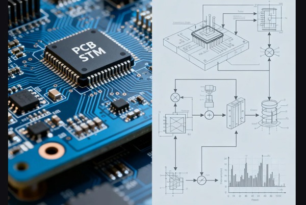
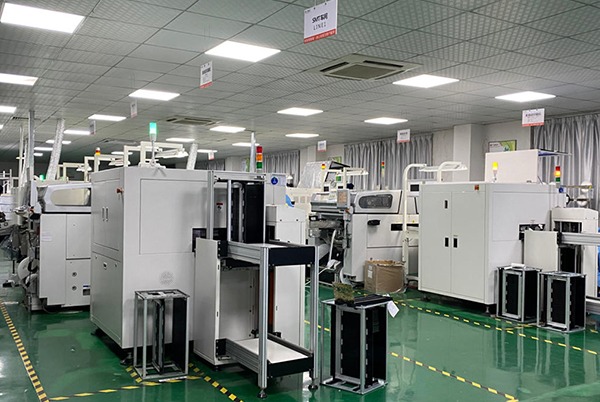
In modern electronics manufacturing, PCB testing is a critical step in ensuring product quality. A single circuit board may contain hundreds of components and thousands of solder joints. Even with a perfect design, various factors in the manufacturing process can lead to functional issues. Systematic testing helps identify problems early, significantly improving yield rates and reducing costs.
Table of Contents
The Importance and Value of PCB Testing
Five Core Benefits of PCB Testing
- Early Defect Detection: Effectively identifies functional and manufacturability issues, providing a basis for design adjustments.
- Production Cost Control: Prototype testing prevents mass production of defective products, reducing material waste.
- Development Cycle Optimization: Identifies major issues during the prototyping phase, shortening time-to-market.
- Quality and Reputation Enhancement: Reduces product return rates and improves customer satisfaction and brand reputation.
- Safety Risk Prevention: Mitigates fire hazards and other safety incidents caused by design flaws, protecting personnel and equipment.
Comprehensive PCB Testing Analysis
PCB testing covers full-spectrum verification from materials to finished products, including the following key items:
- Lamination Quality: Evaluates resistance to delamination under mechanical or thermal stress.
- Hole Wall Integrity: Analyzes resistance to cracking and delamination during thermal cycling.
- Copper Foil Characteristics: Tests tensile strength and elongation of plated copper.
- Environmental Durability: Validates resistance to corrosion, moisture, and other environmental factors.
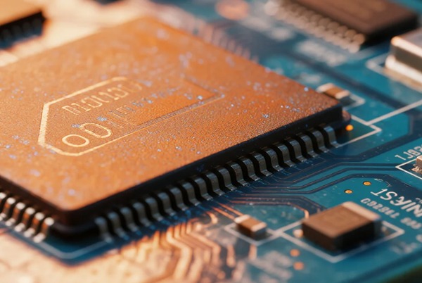
- Solderability: Ensures components can be securely and reliably attached to the board.
- Electrical Properties: Measures conductivity and minimum leakage current.
In-Depth Comparison of 8 Main PCB Testing Methods
1. Manual Visual Inspection
Features: Uses magnification tools to check basic soldering defects.
Advantages: Low cost, simple operation.
Limitations: Relies on inspector experience; cannot evaluate hidden solder joints.
2. Automated Optical Inspection (AOI)
Features: Uses high-resolution cameras for image comparison and analysis.
Advantages: High consistency; can be integrated into production lines.
Limitations: Cannot inspect hidden connections (e.g., under BGAs); time-consuming programming.
3. In-Circuit Testing (ICT)
Features: Uses bed-of-nails probes to verify electrical parameters.
Advantages: Up to 98% fault coverage; ideal for mass production.
Limitations: High fixture costs; unsuitable for frequently changing designs.
4. Flying Probe Testing
Features: Uses movable probes for flexible electrical testing.
Advantages: No need for custom fixtures; high test coverage.
Limitations: Slower testing speed; not ideal for large-scale production.
5. X-Ray Inspection
Features: Inspects hidden solder joints and internal structures via X-ray imaging.
Advantages: Detects solder quality under BGAs and other concealed connections.
Limitations: Requires trained operators; higher costs.
6. Burn-In Testing
Features: Stress-test boards under extreme conditions to assess long-term reliability.
Advantages: Simulates harsh operating environments; screens early failures.
Limitations: May reduce product lifespan; lengthy testing cycles.
7. Functional Testing
Features: Validates performance by simulating real-world operating conditions.
Advantages: Flexible test plans; relatively low cost.
Limitations: Defect detection rate depends on test plan completeness.
8. Boundary Scan Testing
Features: Validates complex IC interconnects using dedicated test chips.
Advantages: Suitable for high-density multilayer boards.
Limitations: Requires boundary scan-compatible components.
Complete PCB Design Inspection Guide
Basic Verification Steps
- File Integrity Check: Confirm the latest design files and manufacturing specifications.
- Electrical Rule Check (ERC): Use EDA tools to verify shorts, opens, and other basic issues.
- Netlist Consistency: Ensure schematics match PCB layouts exactly.
Key Design Review Points
- Component Footprint Verification: Match physical dimensions precisely.
- Power System Evaluation: Ensure current-carrying capacity and network reliability.
- Signal Integrity: Control impedance and crosstalk in high-speed traces.
- Thermal Management: Optimize heat dissipation and component placement.
- EMC Compliance: Validate filtering and shielding effectiveness.
Manufacturability Review
- Process Compatibility: Confirm trace widths, spacing, and other parameters match manufacturer capabilities.
- Test Point Design: Include sufficient test access points.
- Documentation Completeness: Provide detailed assembly drawings and special process instructions.
Recommended Professional Tools
- Use built-in EDA ERC/DRC functions for basic checks.
- Apply signal integrity analysis tools for high-speed designs.
- Leverage DFM analysis software to detect manufacturing issues early.
Continuous Improvement Strategies
- Maintain and update standardized inspection checklists.
- Implement multi-stage design review processes.
- Analyze test data to refine design standards.
By adopting systematic testing strategies and thorough design inspections, PCB product quality and reliability can be significantly improved, reducing production risks and laying a solid foundation for successful electronics.


Related Posts