What equipment do professional PCB manufacturers use?
Table of Contents
Overview of PCB Production Equipment
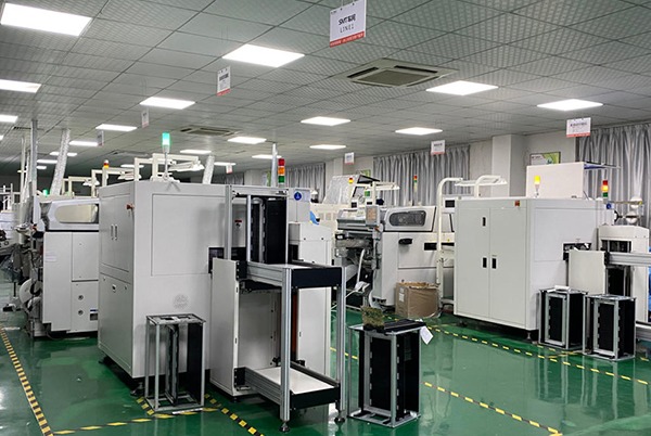
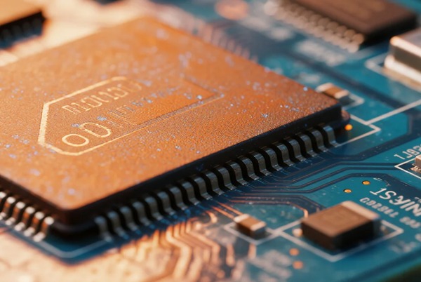
Printed circuit boards (PCBs) are the core components of electronic products, and nearly all electronic devices rely on them. Professional PCB manufacturing plants use a series of high-precision, high-tech equipment to transform design blueprints into actual circuit board products. These machines form the infrastructure of the electronics manufacturing industry, and their technological level directly impacts PCB quality, accuracy, and production efficiency.
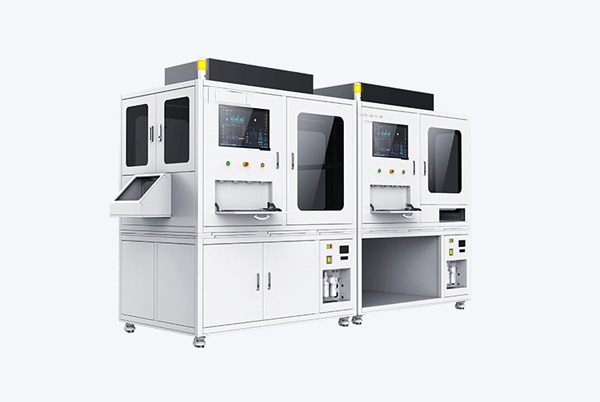
A complete PCB production line consists of dozens of specialized machines, which can be categorized according to the production process into: material preparation equipment, inner layer circuit fabrication equipment, lamination equipment, drilling equipment, plating equipment, outer layer circuit equipment, solder mask and legend printing equipment, and final shaping and testing equipment. Each stage requires specific machinery for precision processing, and any issues in a single step can lead to defective products.
As electronic products trend toward miniaturization and higher density, PCB manufacturing equipment continues to evolve. Modern PCB factories commonly use automated and intelligent production machinery to meet the demands of high precision and consistency. Understanding these specialized machines not only helps electronics engineers design better circuit boards but also assists procurement personnel in evaluating the production capabilities of PCB suppliers.
Material Preparation and Inner Layer Fabrication
The first step in PCB manufacturing begins with the base material. The material preparation workshop is equipped with a series of specialized machines to cut large-sized copper-clad laminates (CCL) into the required dimensions for production. Guillotine shears and panel saws cut large CCL sheets into workable panel sizes with an accuracy of ±0.1 mm. Edge-rounding and edge-grinding machines smooth the panel edges to prevent burrs or delamination in subsequent processes. Cleaning machines and ovens remove surface contaminants and moisture, ensuring stable material quality.
Inner layer circuit fabrication is one of the core stages of PCB production and requires a series of precise imaging transfer equipment. Pre-treatment machines clean the copper surface through chemical and physical methods, enhancing photoresist adhesion. Coating machines evenly apply liquid photoresist to the copper panel to form a photosensitive layer. High-precision exposure machines (such as LDI direct imaging systems) transfer circuit patterns onto the photosensitive layer, with modern equipment achieving line widths below 15 μm. Developing, etching, and stripping machines then permanently fix the circuit pattern onto the copper foil through chemical processes.
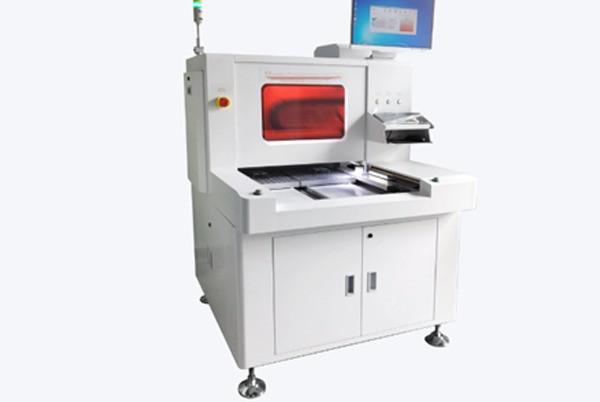
After inner layer fabrication, automated optical inspection (AOI) equipment performs a full scan of the circuitry to detect defects such as open circuits and short circuits. Film measurement tools ensure pattern dimensional accuracy, while panel loaders, unloaders, and dust-removal machines maintain production continuity and cleanliness. Equipment investment at this stage often accounts for more than 20% of the total PCB factory cost, and its technological level directly determines the production capability for high-density interconnect (HDI) boards.
Multilayer Lamination and Precision Drilling
For multilayer PCBs, the lamination workshop is equipped with specialized machinery to bond inner layer cores with prepreg (PP) sheets into a unified structure. PP cutting, trimming, and drilling machines preprocess the prepreg material to ensure layer alignment and uniform resin flow. Brown oxide treatment lines enhance copper surface adhesion. Fusion bonders and riveting machines perform preliminary alignment, while large hydraulic presses (typically over 200 tons of pressure) complete final lamination under high temperature and pressure, with temperature control accuracy within ±1.5°C.
Post-lamination processing is equally critical. X-ray inspection machines check interlayer alignment with an accuracy of ±25 μm. Target milling and CCD drilling machines create reference holes for subsequent processes. Routing machines, edge grinders, and panel cutters perform preliminary shaping, while steel plate cleaners and cooling towers ensure production stability. Multilayer lamination equipment requires substantial investment but is essential for producing high-reliability, high-density circuit boards.
Drilling is one of the most precision-demanding steps in PCB manufacturing. Modern PCB factories use CNC drilling machines equipped with drill bits ranging from 0.1 mm to 6.5 mm, achieving positional accuracy within ±25 μm. Automatic tool-changing systems allow continuous processing of different hole sizes. Drill bit sharpeners extend tool life while pinning and depinning machines handle alignment pins. Hole inspection equipment checks hole wall quality. High-precision drilling is fundamental for ensuring subsequent plating and interconnection quality, especially for HDI boards and IC substrates.
Plating and Outer Layer Circuitry
The plating workshop is one of the “heartbeats” of a PCB factory, responsible for forming reliable conductive pathways. Vertical continuous plating (VCP) and horizontal plating lines (HTP) are mainstream equipment, depositing copper layers on hole walls and surfaces with precise current density control, achieving thickness uniformity within ±10%. Advanced systems like direct metallization (DMSE) activate non-conductive hole walls for subsequent plating. Automated panel handling systems improve production efficiency.
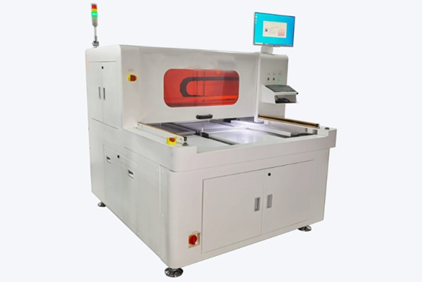
After plating, outer layer circuitry fabrication forms the external circuit patterns. Surface grinders and pretreatment machines clean the copper surface to enhance dry film adhesion. Lamination machines apply photosensitive dry film, while high-precision exposure systems (such as laser direct imaging) transfer outer layer patterns with resolutions up to 20 μm. Developing, etching, and stripping lines remove excess copper foil, forming precise circuit patterns. In-line AOI systems perform full inspections to ensure no open circuits, short circuits, or other defects.
After outer layer fabrication, preliminary electrical testing is conducted in the electrical test (ET) department. AOI scanners and flying probe testers check circuit connectivity. Rework stations and line repair machines fix minor defects while punching machines create tooling holes. Equipment at this stage requires extreme stability and consistency, as outer layer circuits directly connect to components and affect final product performance.
Surface Finishing and Final Processing
Solder mask (resist) application protects circuits and prevents soldering shorts. Pretreatment grinders clean copper surfaces before a liquid photo imageable solder mask (LPSM) is applied via screen printing or spraying, with thickness control within ±5 μm. Exposure machines define opening areas using films or LDI technology, and developers remove the uncured resist. Modern factories use automated visual inspection (AVI) systems to check solder mask quality, while ultrasonic cleaners ensure surface cleanliness. Convection ovens and IR tunnels cure the resist with precise temperature profiling.
Legend printing adds identification markings. Traditional screen printing remains common, but digital inkjet printing is gaining popularity, producing clear sub-0.5 mm characters. Screen preparation areas include emulsion coating, washing, and exposure machines to ensure print quality. IR ovens and curing tunnels harden legend ink to prevent peeling during later processes.
The routing department separates panels into individual boards and processes edges. CNC routers (milling machines) cut complex outlines with ±0.05 mm accuracy. V-scoring machines handle breakaway tab designs, while punch presses suit high-volume simple shapes. Cleaning machines remove debris for spotless finished products.
The final test department performs electrical verification. Flying probe testers suit low-volume, high-complexity boards, whereas bed-of-nails testers handle mass production, testing in seconds per board. Final inspection ensures compliance with all customer requirements. Thickness gauges check uniformity, flattening machines improve planarity, and manual/automated visual inspection provides last-minute defect screening. Organic solderability preservative (OSP) lines treat exposed pads to enhance solderability.
The packaging uses anti-static materials to prevent shipping damage. The entire PCB production equipment setup requires massive investment but is essential for manufacturing high-quality circuit boards.


Related Posts